

Sort by

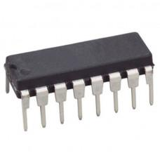
CD4016 - Quad Bilateral Switc…
CD4016 - Quad Bilateral Switch IC
The
CD4x Series
CD4016 is a quad bilateral switch intended for the transmission or multiplexing of analog or digital signals. It is pin-for-pin compatible with CD4066B.
The CD4016 is a CMOS IC with four analog switches, which can be controlled individually using a control pin. The signal can flow in either direction between the two pins of each switch.
Each switch has an enable pin (A) and two input/output pins (X and Y). When the enable pin is set to HIGH, current can flow between X and Y in either direction. However, when enable is LOW, no current can flow between the pins. Just like a switch.
Pinout:
Pinout of CD4016 IC
Pin Name
Pin #
Type
Description
VDD
14
Power
Supply Voltage (+3 to +15V)
GND
7
Power
Ground (0V)
A1-A4
5,6,12,13
Input
Enable pins for the four bilateral switches
X1-X4
1,3,9,11
Input/Output
Pin X for each switch
Y1-Y4
2,4,8,10
Input/Output
Pin Y for each switch
₹24,49
MRP. ₹47,60
Incl. GST (No Hidden Charges)
Incl. GST (No Hidden Charges)

CD4016 - Quad Bilateral Switch IC
CD4016 - Quad Bilateral Switch IC The CD4x Series CD4016 is a quad bilateral switch intended for the transmission or multiplexing of analog or digital signals. It is pin-for-pin compatible …
As low as
₹24,49
₹24,49
MRP. ₹47,60
Incl. GST (No Hidden Charges)
CD4017 - Decade Counter IC
CD4017 - Decade Counter IC
The CD4017
IC
is a
decade counter
that counts to ten. It has 10 outputs that represent the numbers 0 to 9. The counter increases with one for every rising clock pulse. After the counter has reached 9, it starts again from 0 with the next clock pulse.
This is a great chip for making running LEDs! See a circuit example further down.
check out :
Dual Complementary Pair with Inverter IC - CD4007
Pin Overview:
Pinout of CD4017 - Decade Counter IC
Pin Name
Pin #
Type
Description
VDD
16
Power
Supply Voltage (+3 to +15V)
GND
8
Power
Ground (0V)
Q0-Q9
1-7 and 9-11
Output
Qx is high when the counter is x
CO
12
Output
Carry Out. Goes high after ten clock pulses
CI
13
Input
Clock Inhibit. Ignores clock inputs
CLK
14
Input
Clock Input. Increases the counter with one
MR
15
Input
Resets the counter to 0
₹14,47
MRP. ₹25,20
Incl. GST (No Hidden Charges)
Incl. GST (No Hidden Charges)


CD4017 - Decade Counter IC
CD4017 - Decade Counter IC The CD4017 IC is a decade counter that counts to ten. It has 10 outputs that represent the numbers 0 to 9. The counter increases …
As low as
₹14,47
₹14,47
MRP. ₹25,20
Incl. GST (No Hidden Charges)
CD4028 - BCD to Decimal Decod…
CD4028 - BCD to Decimal Decoder IC
CD4028 IC is a BCD to decimal or binary to octal decoder consisting of 4 inputs and 10 output buffers. A BCD code is applied to the 4 inputs, A, B, C, and D. Thus resulting in a high level at the selected 1-of-10 decimal decoded outputs. Similarly, a 3-bit binary code applied to inputs A, B, and C is decoded into octal at outputs 0–7. A high-level signal at the D input inhibits octal decoding and causes outputs 0–7 to go LOW.
The
IC
is always available in a 16–pin hermetically sealed dual inline IC package (DIP), making it easy to interface with TTL, CMOS, and NMOS devices. The IC offers many features such as high noise immunity and low thermal dissipation. High drive capability is provided at all outputs to enhance dc and dynamic performance in high fan- ut applications. Meanwhile, all the inputs are protected against static discharge damage by diode clamps to V
DD
and V
SS
.
A BCD to Decimal Decoder is defined as a simple logic circuit that can translate a BCD (binary coded decimal) input into a decimal (0 – 9) output In any BCD to decimal decoder, the inverters are connected in pairs to make BCD input data available for decoding by the NAND gates. Full decoding of valid BCD input logic ensures that all outputs remain OFF for all invalid binary input conditions. Moreover, these decoders feature TTL inputs and high–performance NPN output transistors designed for use as indicator/relay drivers or as open–collector logic circuit drivers.
check out :
CD4514 - 4 Bit Latch/4-16 Line Decoder IC
Pinout:
Pinout of CD4028 IC
Application
Code conversion
Address decoding
Indicator-tube decoder
₹22,25
MRP. ₹47,60
Incl. GST (No Hidden Charges)
Incl. GST (No Hidden Charges)

CD4028 - BCD to Decimal Decoder IC
CD4028 - BCD to Decimal Decoder IC CD4028 IC is a BCD to decimal or binary to octal decoder consisting of 4 inputs and 10 output buffers. A BCD code …
As low as
₹22,25
₹22,25
MRP. ₹47,60
Incl. GST (No Hidden Charges)
CD4029 - Binary Decade Up-Dow…
CD4029 - Binary Decade Up-Down Counter IC
The CD4029 IC consists of a four-stage binary or BCD-decade up/ down counter with provisions for look-ahead carry in both counting modes. The inputs consist of a single CLOCK, CARRY-IN (CLOCK ENABLE), BINARY/DECADE, UP/DOWN, PRESET ENABLE, and four individual JAM signals. Q1, Q2, Q3, Q4, and a CARRY OUT signal are provided as outputs.
A high PRESET ENABLE signal allows information on the JAM INPUTS to preset the counter to any state asynchronously with the clock. A low on each JAM line, when the PRESET-ENABLE signal is high, resets the counter to its zero counts. The counter is advanced one count at the positive transition of the clock when the CARRY-IN and PRE-SET ENABLE signals are low. Advancement is inhibited when the CARRY-IN or PRESET ENABLE signals are high. The CARRY-OUT signal is normally high and goes low when the counter reaches its maximum count in the UP mode or the minimum count in the DOWN mode provided the CARRY-IN signal is low. The CARRY-IN signal in the low state can thus be considered a CLOCK ENABLE.
The CARRY-IN terminal must be connected to VSS when not in use. Binary counting is accomplished when the BINARY/DECADE input is high; the counter counts in the decade mode when the BINARY/DECADE input is low. The counter counts up when the UP/DOWN input is high, and down when the UP/DOWN input is low. Multiple packages can be connected in either a parallel clocking or a ripple-clocking arrangement as shown in Figure 17. Parallel clocking provides synchronous control and hence faster response from all counting outputs. Ripple-clocking allows for longer clock input rise and fall times. The
CD4x Series
CD4029 is supplied in these 16-lead outline packages: Braze Seal DIP H4X Frit Seal DIP H1F Ceramic Flatpack H6W.
Pinout:
Pinout of CD4029 IC
₹42,28
MRP. ₹61,60
Incl. GST (No Hidden Charges)
Incl. GST (No Hidden Charges)

CD4029 - Binary Decade Up-Down Counter IC
CD4029 - Binary Decade Up-Down Counter IC The CD4029 IC consists of a four-stage binary or BCD-decade up/ down counter with provisions for look-ahead carry in both counting modes. The …
As low as
₹42,28
₹42,28
MRP. ₹61,60
Incl. GST (No Hidden Charges)
CD4030 - Quad 2-Input Exclusi…
CD4030 - Quad 2-Input Exclusive OR (EXOR) Gate IC
The CD4030
IC
types consist of four independent Exclusive-OR gates. The CD4030 provides the system designer with a means for direct implementation of the Exclusive-OR function.
The CD4030 types are supplied in 14-lead hermetic dual-in-line ceramic packages (F3A suffix), 14-lead dual-in-line plastic packages (E suffix), 14-lead small-outline packages (M, MT, M96, and NSR suffixes), and 14-lead thin shrink small-outline packages (PW and PWR suffixes).
check out :
CD4519 - Quad AND/OR Select Gate IC (Original)
Pinout:
Pinout of CD4030 - Quad 2-Input Exclusive OR (EXOR) Gate IC
Applications:
Even and odd-parity generators and checkers
Logical comparators
Adders/subtractors
General logic functions
check out :
CD4081 - Quad 2 Input AND Gate IC
₹25,59
MRP. ₹50,40
Incl. GST (No Hidden Charges)
Incl. GST (No Hidden Charges)

CD4030 - Quad 2-Input Exclusive OR (EXOR) Gate IC
CD4030 - Quad 2-Input Exclusive OR (EXOR) Gate IC The CD4030 IC types consist of four independent Exclusive-OR gates. The CD4030 provides the system designer with a means for direct …
As low as
₹25,59
₹25,59
MRP. ₹50,40
Incl. GST (No Hidden Charges)
CD4033 - 5-Stage Johnson Deca…
CD4033 - 5-Stage Johnson Decade counter IC
The CD4033
IC
consists of a 5-stage Johnson decade counter IC and an output decoder that converts the Johnson code to a 7-segment decoded output for driving one stage in a numerical display.
These devices are particularly advantageous in display applications where low power dissipation and /or low package count are important.
Inputs common to both types are CLOCK, RESET, & CLOCK INHIBIT; common outputs are CARRY OUT and the seven decoded outputs (a, b, c, d, e, f, g). Signals peculiar to the CD4033 are RIPPLE-BLANKING INPUT AND LAMP TEST INPUT and a RIPPLE-BLANKING OUTPUT.
A high RESET signal clears the decade counter to its zero counts. The counter is advanced one count at the positive clock signal transition if the CLOCK INHIBIT signal is low. Counter advancement via the clock line is inhibited when the CLOCK INHIBIT signal is high. The CLOCK INHIBIT signal can be used as a negative-edge clock if the clock line is held high. Anti-lock gating is provided on the JOHNSON counter, thus assuring proper counting sequence. The CARRY-OUT (C
out
) signal completes one cycle every ten CLOCK INPUT cycles and is used to clock the succeeding decade directly in a multi-decade counting chain. The seven decoded outputs (a, b, c, d, e, f, g) illuminate the proper segments in a seven-segment display device used for representing the decimal numbers 0 to 9. The 7-segment outputs go high on selection in the CD4033.
The CD4033 series types are supplied in 16-lead dual-in-line plastic packages (E suffix), 16-lead small-outline packages (NSR suffix), and 16-lead thin shrink small-outline packages (PW and PWR suffixes).
Pinout:
Pinout of CD4033 - 5-Stage Johnson Decade counter IC
Pin 1 known as Clock in
– It receives clock signals, and at every positive clock counter advances one by one. You can provide a clock with the switch, 555 timer or the help of logic gates.
Pin 2 known as Clock inhibit
– CD4033 counter advances one by one by receiving a positive pulse at this time clock inhibit pin should be grounded. If it is connected to the supply then counter advancement will be inhibited means there will be no meaning of clock pulse.
Pin 3 and pin 4 known as Ripple blanking in and Ripple blanking
– It is used to display only one zero blanking the other zero. For this IC have ripple blanking in and ripple blanking out. For example, you want to display 345 and you are using five 7 segment display then it will display 00345 if blanking input and out is off. But if it is on then you will receive 345. It improves the readability of the circuit.
Pin 5 known as carry out
– It is used to complete one cycle for every 10-clock input cycle and it is also used to cascade more ICs.
Pin 6, pin7 and Pin9 to pin 13
– These are 7 decoded outputs from a to g used to illuminate the corresponding segment of 7 segment display to display the digit from 0 to 9.
Pin 14 known as Lamp test
– t is used to check whether all segments of 7 segment is working properly or not. For testing momentarily make the pin low.
Pin 15 known as
Reset
– It is used to reset the counter. When it receives high it clears the counter and counting again starts from zero. One important thing reset pin should again made low to start the counter once again.
Pin 8 known as ground
pin and
Pin 16 known as Vdd
it should be connected to power supply.
Applications:
Decade counting 7-segment decimal display
Frequency division 7-segment decimal displays
Clocks, watches, timers (e.g. ÷60, ÷60, ÷ 12 counter/display)
Counter/display driver for meter applications
check out :
CD4060 - 14 stage Ripple Carry Binary Counter IC
₹240,35
MRP. ₹348,60
Incl. GST (No Hidden Charges)
Incl. GST (No Hidden Charges)
CD4033 - 5-Stage Johnson Decade counter IC
CD4033 - 5-Stage Johnson Decade counter IC The CD4033 IC consists of a 5-stage Johnson decade counter IC and an output decoder that converts the Johnson code to a 7-segment …
As low as
₹240,35
₹240,35
MRP. ₹348,60
Incl. GST (No Hidden Charges)
CD4034 - 8-Stage Bidirectiona…
CD4034 - 8-Stage Bidirectional Bus Register IC
The CD4034 Register
IC
is a static eight-stage parallel-or serial-input parallel-output register. It can be used to:
1) Bi-directionally transfer parallel information between two buses, 2) convert serial data to parallel form and direct the parallel data to either of two buses, 3) store (recirculate) parallel data, or 4) accept parallel data from either of two buses and convert that data to serial form. Input that controls the operations includes a single-phase CLOCK (CL), A-DATA ENABLE (AE), ASYNCHRONOUS/SYNCHRONOUS (A/S), A-BUS-TO-B-BUS/B-BUS-TO-A-BUS (A/B), and PARALLEL/SERIAL (P/S).
Data inputs include 16 bidirectional parallel data lines of which the eight A data lines are inputs (3-state outputs) and the B data lines are outputs (inputs) depending on the signal level on the A/B input. In addition, input for SERIAL DATA is also provided.
All register stages are D-type master-slave flip-flops with separate master and slave clock inputs generated internally to allow synchronous or asynchronous data transfer from master to slave. Isolation from external noise and the effects of loading is provided by output buffering.
Register expansion can be accomplished by simply cascading CD4034 packages.
The CD4034 types are supplied in 24-lead hermetic dual-in-line ceramic packages (F3A suffix), 24-lead dual-in-line plastic packages (E suffix), 24-lead small-outline packages (M, M96, and NSR suffixes), and 24-lead thin shrink small-outline packages (PW and PWR suffixes).
Pinout:
Pinout of CD4034 - 8-Stage Bidirectional Bus Register IC
Applications:
Parallel Input/Parallel Output, Serial Input/Parallel Output, Serial Input/Serial Output Register
Shift right/shift-left register
Shift right/shift left with parallel loading
Address register
Buffer register
Bus system register with enable parallel lines at bus side
Double bus register system
Up-Down Johnson or ring counter
Pseudo-random code generators
Sample and hold register (storage, counting, display)
Frequency and phase comparator
₹109,04
MRP. ₹197,40
Incl. GST (No Hidden Charges)
Incl. GST (No Hidden Charges)

CD4034 - 8-Stage Bidirectional Bus Register IC (Original)
CD4034 - 8-Stage Bidirectional Bus Register IC The CD4034 Register IC is a static eight-stage parallel-or serial-input parallel-output register. It can be used to: 1) Bi-directionally transfer parallel information between …
As low as
₹109,04
₹109,04
MRP. ₹197,40
Incl. GST (No Hidden Charges)
CD4040 - 12-Stage Ripple Carr…
CD4040 - 12-Stage Ripple Carry Binary Counter IC
The
CD4x Series
CD4040 is a ripple-carry binary counter that features 12 stages, push-pull type, and balanced outputs, with standard speed (TPD > 50ns). All counter stages are master-slave flip-flops. Supports wide input voltage ranges from 3V to 18V. The maximum input current at 18V is 1 uA whereas 100 nA at 18V and 25°C.
All counter stages are master-slave flip-flops. The state of a counter advances one count on the negative transition of each input pulse; a high level on the RESET line resets the counter to its all-zeros state. Schmitt's trigger action on the input-pulse line permits unlimited rise and fall times. All inputs and outputs are buffered. 16 Pin DIP is available in a hermetic dual-in-line ceramic package.
We also have a
CD4020
with similar features. The differences are CD4020 is a 14 Stage binary counter whereas CD4040 is a 12 Stage binary counter and there is a difference between the pin layout.
check out :
CD4518 - Dual BCD Up Counter IC (Original)
Pinout:
Pinout of CD4040 IC
Applications:
Control Counters
Timers
Frequency Dividers
Time-Delay Circuits
₹31,15
MRP. ₹47,60
Incl. GST (No Hidden Charges)
Incl. GST (No Hidden Charges)
CD4040 - 12-Stage Ripple Carry Binary Counter IC
CD4040 - 12-Stage Ripple Carry Binary Counter IC The CD4x Series CD4040 is a ripple-carry binary counter that features 12 stages, push-pull type, and balanced outputs, with standard speed (TPD …
As low as
₹31,15
₹31,15
MRP. ₹47,60
Incl. GST (No Hidden Charges)
CD4046 - Micropower Phase Loc…
CD4046 - Micropower Phase Locked Loop IC
CD4046 CMOS Micropower Phase-Locked Loop (PLL) IC consists of a low-power, linear voltage-controlled oscillator (VCO) and two different phase comparators having a common signal-input amplifier and a common comparator input. A 5.2-V Zener diode is provided for supply regulation if necessary.
The
CD series
CD4046 types are supplied in 16-lead hermetic dual-in-line ceramic packages (F3A suffix), 16-lead dual-in-line plastic packages (E suffix), 16-lead small-outline packages (NSR suffix), and 16-lead thin shrink small-outline packages (PW and PWR suffixes).
check out :
Dual JK Flip Flop IC - CD4027
Pinout:
Pinout of CD4046 IC
Applications:
FM demodulator and modulator
Frequency synthesis and multiplication
Frequency discriminator
Data synchronization
Voltage-to-frequency conversion
Tone decoding
FSK - Modems
Signal conditioning
₹30,04
MRP. ₹50,40
Incl. GST (No Hidden Charges)
Incl. GST (No Hidden Charges)

CD4046 - Micropower Phase Locked Loop IC
CD4046 - Micropower Phase Locked Loop IC CD4046 CMOS Micropower Phase-Locked Loop (PLL) IC consists of a low-power, linear voltage-controlled oscillator (VCO) and two different phase comparators having a common …
As low as
₹30,04
₹30,04
MRP. ₹50,40
Incl. GST (No Hidden Charges)
CD4047 - Astable/Monostable M…
CD4047 - Astable/Monostable Multivibrator IC
CD4047
IC
consists of a gateable astable multivibrator with logic techniques incorporated to permit positive or negative edge-triggered monostable multivibrator action with retriggering and external counting options.
Inputs include +TRIGGER, -TRIGGER, ASTABLE, ASTABLE\, RETRIGGER, and EXTERNAL RESET. Buffered outputs are Q\, Q an OSCILLATOR. In all modes of operation, an external capacitor must be connected between C-Timing and RC-Common terminal, and an external resistor must be connected between the R-Timing and RC-Common terminals.
Astable operation is enabled by a high level on the STABLE input or a low level on the ASTABLE\ input, or both. The period of the square wave at the Q and Q\ Outputs in this mode of operation is a function of the external components employed. "True" input pulses on the ASTABLE input or "Complement" pulses on the ASTABLE\ input allow the circuit to be used as a gateable multivibrator. The OSCILLATOR output period will be half of the Q terminal output in the astable mode. However, a 50% duty cycle is not guaranteed at this output.
The CD4047 triggers in the monostable mode when a positive-going edge occurs on the +TRIGGER-input while the -TRIGGER is held low. Input pulses may be of any duration relative to the output pulse.
The CD4047-Series types are supplied in 14-lead hermetic dual-in-line ceramic packages (F3A suffix), 14-lead dual-in-line plastic packages (E suffix), 14-lead small-outline packages (M, MT, M96, and NSR suffixes), and 14-lead thin shrink small-outline packages (PW and PWR suffixes).
check out :
CD4094 - 8-Stage Shift and Store Bus Register IC
Pinout:
Pinout of CD4047 IC
Applications:
Digital equipment where low-power dissipation and/or high noise immunity are primary design requirements:
Envelope detection
Frequency multiplication
Frequency division
Frequency discriminators
Timing circuits
Time-delay applications
₹24,49
Incl. GST (No Hidden Charges)
Out of Stock
MRP. ₹49,00
Incl. GST (No Hidden Charges)

CD4047 - Astable/Monostable Multivibrator IC
CD4047 - Astable/Monostable Multivibrator IC CD4047 IC consists of a gateable astable multivibrator with logic techniques incorporated to permit positive or negative edge-triggered monostable multivibrator action with retriggering and external …
As low as
₹24,49
₹24,49
MRP. ₹49,00
Incl. GST (No Hidden Charges)
Out of Stock
