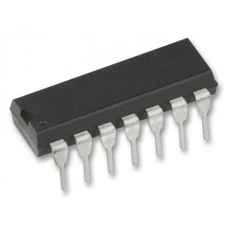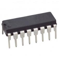
CD4033 - 5-Stage Johnson Decade counter IC
Delivery & Pickup Options
Order now and we'll have it ready for delivery by the next business day.
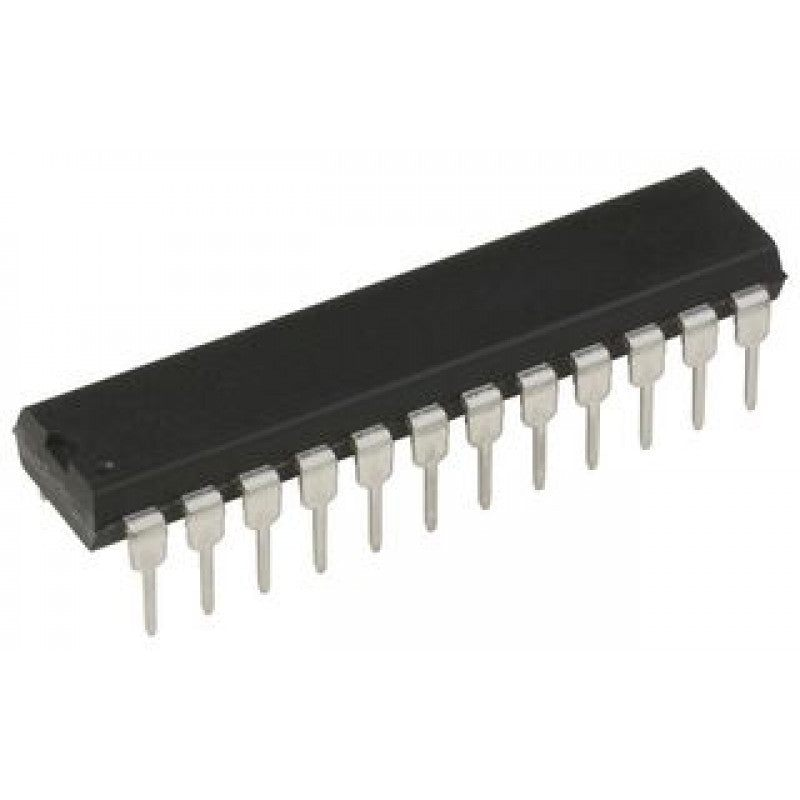
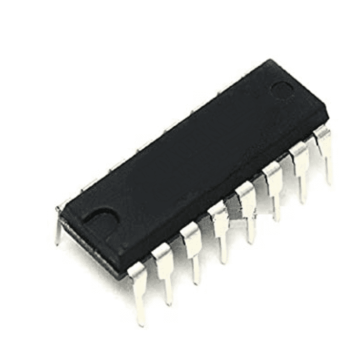
CD4033 - 5-Stage Johnson Decade counter IC The CD4033 IC consists of a 5-stage Johnson decade counter IC and an output decoder that converts the Johnson code to a 7-segment decoded output for driving one stage in a numerical display. These devices are particularly advantageous in display applications where low power dissipation and /or low package count are important. Inputs common to both types are CLOCK, RESET, & CLOCK INHIBIT; common outputs are CARRY OUT and the seven decoded outputs (a, b, c, d, e, f, g). Signals peculiar to the CD4033 are RIPPLE-BLANKING INPUT AND LAMP TEST INPUT and a RIPPLE-BLANKING OUTPUT. A high RESET signal clears the decade counter to its zero counts. The counter is advanced one count at the positive clock signal transition if the CLOCK INHIBIT signal is low. Counter advancement via the clock line is inhibited when the CLOCK INHIBIT signal is high. The CLOCK INHIBIT signal can be used as a negative-edge clock if the clock line is held high. Anti-lock gating is provided on the JOHNSON counter, thus assuring proper counting sequence. The CARRY-OUT (C out ) signal completes one cycle every ten CLOCK INPUT cycles and is used to clock the succeeding decade directly in a multi-decade counting chain. The seven decoded outputs (a, b, c, d, e, f, g) illuminate the proper segments in a seven-segment display device used for representing the decimal numbers 0 to 9. The 7-segment outputs go high on selection in the CD4033. The CD4033 series types are supplied in 16-lead dual-in-line plastic packages (E suffix), 16-lead small-outline packages (NSR suffix), and 16-lead thin shrink small-outline packages (PW and PWR suffixes). Pinout: Pinout of CD4033 - 5-Stage Johnson Decade counter IC Pin 1 known as Clock in – It receives clock signals, and at every positive clock counter advances one by one. You can provide a clock with the switch, 555 timer or the help of logic gates. Pin 2 known as Clock inhibit – CD4033 counter advances one by one by receiving a positive pulse at this time clock inhibit pin should be grounded. If it is connected to the supply then counter advancement will be inhibited means there will be no meaning of clock pulse. Pin 3 and pin 4 known as Ripple blanking in and Ripple blanking – It is used to display only one zero blanking the other zero. For this IC have ripple blanking in and ripple blanking out. For example, you want to display 345 and you are using five 7 segment display then it will display 00345 if blanking input and out is off. But if it is on then you will receive 345. It improves the readability of the circuit. Pin 5 known as carry out – It is used to complete one cycle for every 10-clock input cycle and it is also used to cascade more ICs. Pin 6, pin7 and Pin9 to pin 13 – These are 7 decoded outputs from a to g used to illuminate the corresponding segment of 7 segment display to display the digit from 0 to 9. Pin 14 known as Lamp test – t is used to check whether all segments of 7 segment is working properly or not. For testing momentarily make the pin low. Pin 15 known as Reset – It is used to reset the counter. When it receives high it clears the counter and counting again starts from zero. One important thing reset pin should again made low to start the counter once again. Pin 8 known as ground pin and Pin 16 known as Vdd it should be connected to power supply. Applications: Decade counting 7-segment decimal display Frequency division 7-segment decimal displays Clocks, watches, timers (e.g. ÷60, ÷60, ÷ 12 counter/display) Counter/display driver for meter applications check out : CD4060 - 14 stage Ripple Carry Binary Counter IC
- Counter and 7-segment decoding in one package
- Easily interfaced with 7-segment display types
- Fully static counter operation: DC to 6 MHz (typ.) at VDD = 10 V
- Ideal for low-power displays
- Display enable output (CD4026B)
- “Ripple blanking” and lamp test (CD4033B)
- 100% tested for quiescent current at 20 V
- Standardized, symmetrical output characteristics
- 5-V, 10-V, and 15-V parametric ratings
- Schmitt-triggered clock inputs
- Meets all requirements of JEDEC Tentative Standard No. 13B, “Standard Specifications for Description of ’B’ Series CMOS Devices”
- Part number CD4033B
- Technology Family CD4000
- VCC (Min) (V) 3
- VCC (Max) (V) 18
- Bits (#) 7
- Voltage (Nom) (V) 5, 10, 15
- F @ nom voltage (Max)(MHz) 8
- ICC @ nom voltage (Max)(mA) 0.03
- tpd @ nom Voltage (Max)(ns) 250
- IOL (Max) (mA) 1.5
- IOH (Max) (mA) -1.5
- Function Counter
- Type Decade
- Rating See Data Sheet
- Operating temperature range (C) -55 to 125
- Package Group PDIP|16