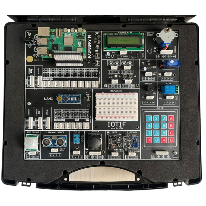
(0)
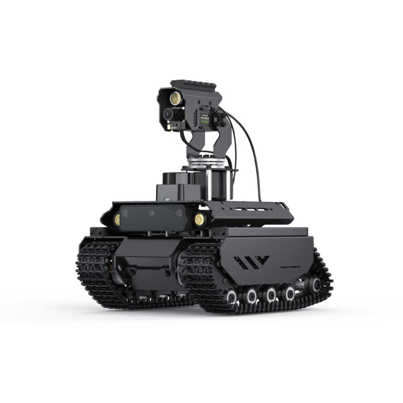
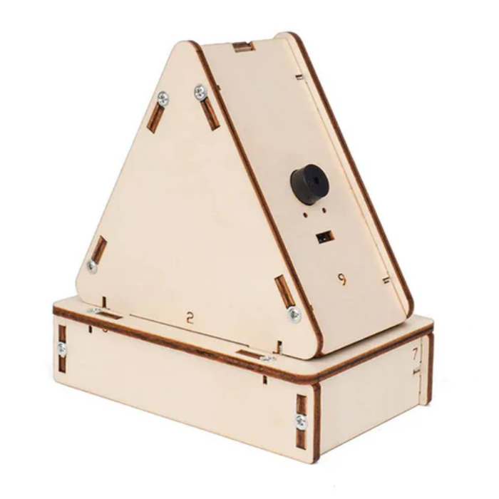
Waveshare UGV Beast Open-source Off-Road AI Robot Chassis Kit with Raspberry Pi 4B and Pan Tilt - PT PI4B ROS2
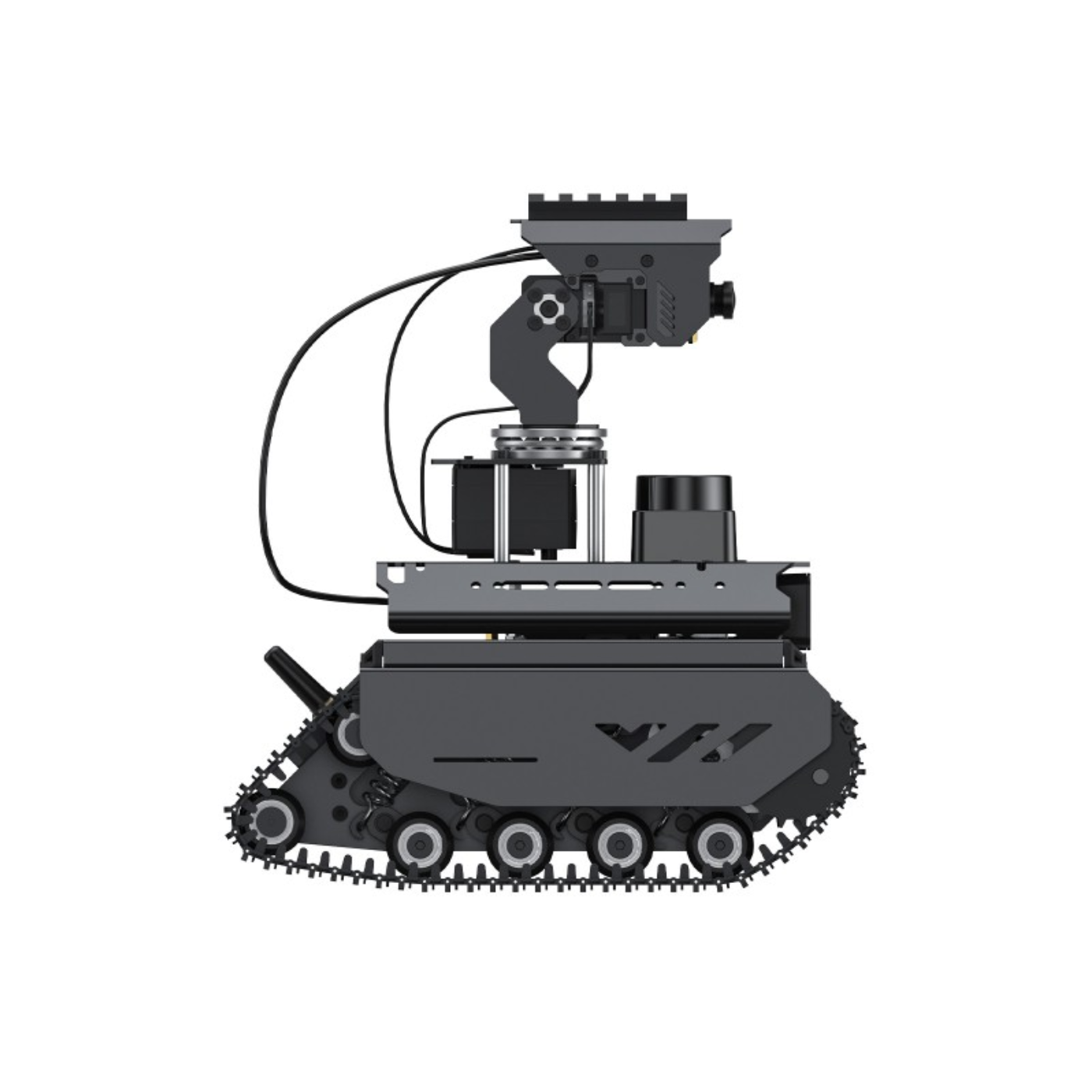
The UGV Beast ROS2 Kit is a cutting-edge AI robot designed for those interested in exploration, creation, and robotics. Built on ROS 2, it comes equipped with a Lidar and depth camera, making it perfect for both tech enthusiasts and beginners looking to dive into intelligent technology. With its dual-controller design, it combines the power of a host controller for high-level AI functions and a sub-controller for high-frequency operations, ensuring smooth and accurate performance in all tasks.
The UGV Beast is easily controlled remotely through a web application—no software installation required—allowing users to begin their journey simply by opening a browser. This robot supports real-time high-frame rate video and a range of AI Computer Vision capabilities, making it an ideal platform to test and bring creative ideas to life. Powered by a Raspberry Pi, the UGV Beast provides the computational power needed for complex functions and exploration, offering endless opportunities to realize your innovative concepts.
Features:
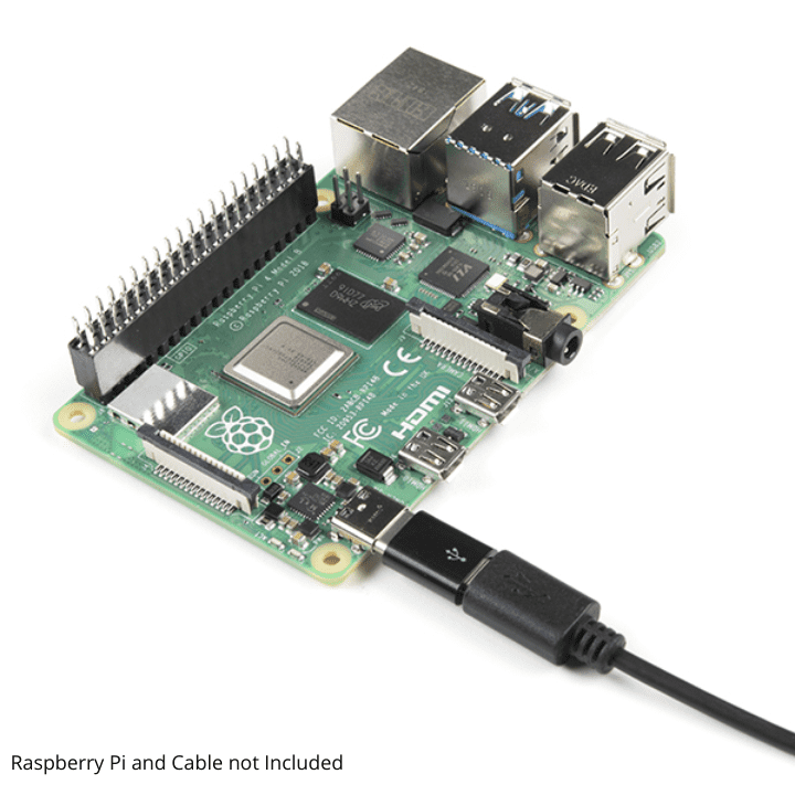
Based on Raspberry Pi
Supports Raspberry Pi 4B, with powerful computing performance to handle more complex tasks, offering more possibilities
Dual-Controller Architecture Offers Improved Performance and Effective Teamwork.
The sub controller employs an ESP32 for motion control and sensor data processing, while the host controller uses a Raspberry Pi for AI vision and strategy planning.
Raspberry Pi OS + ROS2 Docker
Guarantees both system compatibility and the robot's enhanced decision-making performance. All AI features of the earlier AI Kit series products are supported.
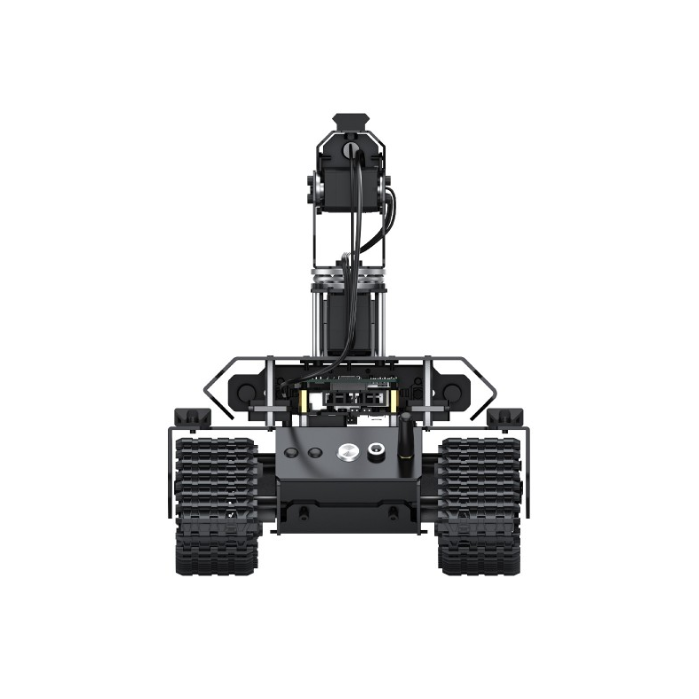
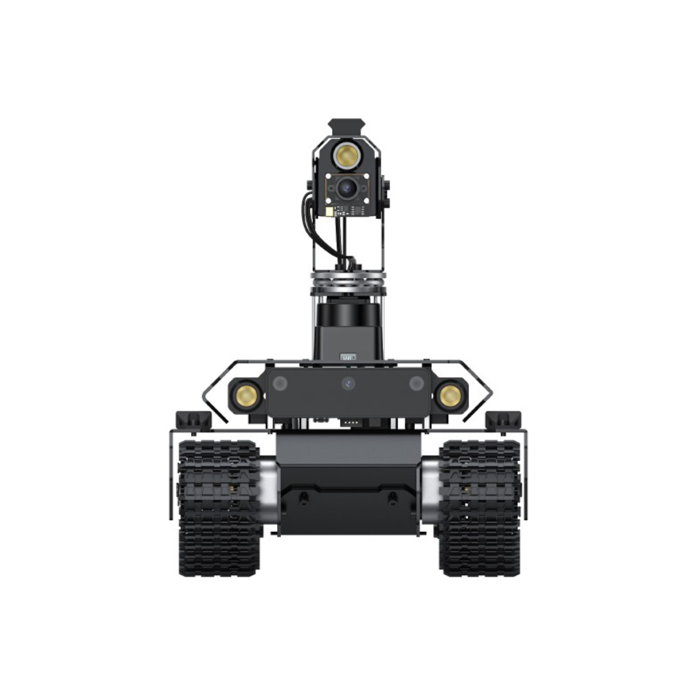
360° Flexible Omnidirectional Pan-Tilt
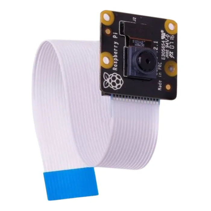
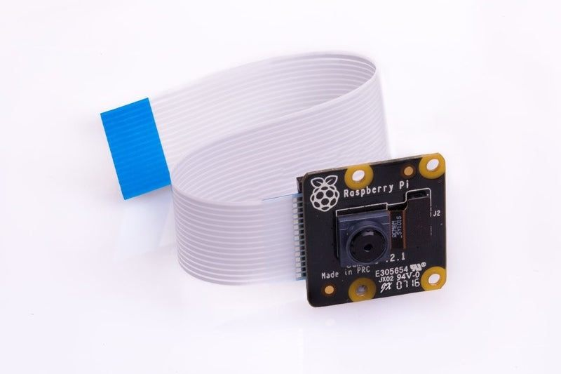
equipped with 5MP 160° wide-angle camera for capturing every detail
All ROS 2 Development Resources are Free Source.
All host controller and sub controller demonstrations, including the robot description file (URDF model), the sub controller's sensor data processing node, kinematic control algorithms, and several remote-control nodes, are open source.
Multiple Cost-Effective Sensors
Adopts multiple sensors with high cost-effectiveness and practicality
Auto-Exploration and Mapping
Implementing mapping and navigation features concurrently in unfamiliar locations Ising SLAM Toolbox, which streamlines the task execution method. Unmanned applications can benefit from the UGV robot's ability to map and explore new places on its own.
Facilitates Communication with Natural Language
By using large language model (LLM) technology, users may command the robot using natural language, allowing it to carry out activities including mapping, navigation, and movement.
Offers a Web Console Tool
Without setting up a virtual machine on your computer, you may use the basic ROS 2 features online. It also works cross-platform on tablets running iOS or Android. To move, map, navigate, and perform other tasks, users only need to launch a web browser.
As Night Falls, the Adventure Continues, Supporting Tactical Extension
LED light with high brightness to ensure sharp images in low light
Recognition, Tracking, and Targeting
Built on OpenCV to do automatic targeting and color recognition. allows for extension for additional functionalities and supports automatic LED illumination and one-key pan-tilt control.
Other Features:
Supports Various ROS 2 Mapping Methods:
Meet the needs of mapping in different scenarios
ROS2 node command interaction:
Users can send control commands via script for operations like moving, location tracking, and navigation, enabling convenient secondary development.
Gazebo simulation debugging:
Offers Gazebo robot mode and a complete functionality library for simulation debugging, helping verify and test the system in early development stages.
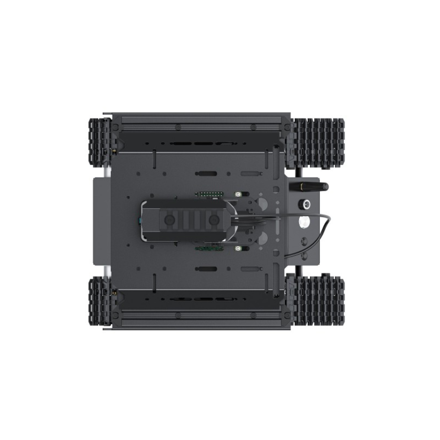
Standard Aluminum rail:
Includes 2 × 10²⁰ European standard profile rails and allows for the easy expansion of specific operation situations by adding more peripherals via the boat nuts to suit various needs.
Supports driving in complex terrain:
Enables more stable off-road crossing by utilizing tracked mobile robot chassis with independent suspension systems.
Easy Control via Web App:
No app needed control via browser on mobile, tablet, or PC with keyboard shortcuts like WASD and mouse support.
WebRTC real-time video transmission:
Flask-based lightweight web app with WebRTC for ultra-low latency, Python-powered, easily extendable, and OpenCV compatible.
Face Detection & Auto Capture:
Based on OpenCV to achieve Face recognition, supports automatic photo taking or video recording once a face is recognized.
Intelligent Object Recognition:
Supports recognizing for many common objects with the default model.
Gesture Recognition: AI-Powered Body Interaction:
Combines OpenCV and Media Pipe to realize gesture control of Pan-Tilt and LED.
More Media Pipe Demos for Easy Video Processing:
MediaPipe, an open-source framework by Google, enables high-performance multimedia processing for real-time video analytics in robotics.
40PIN GPIO Extended Header:
The robot uses only the Raspberry Pi UART GPIO for communication while providing a 40PIN header for peripheral expansion.
Real-Time Data Feedback:
Real-time monitoring the operating status of the robot.
Web Command Line Tool with Expandable Functions:
Quick to set up, easy to expand
Easily customize and add new functions without Modifying front-end code.
ESP-NOW Wireless Communication for Robots:
Using the ESP-NOW protocol, multiple robots can communicate without IP/MAC addresses, enabling multi-device collaboration with 100-microsecond low-latency.
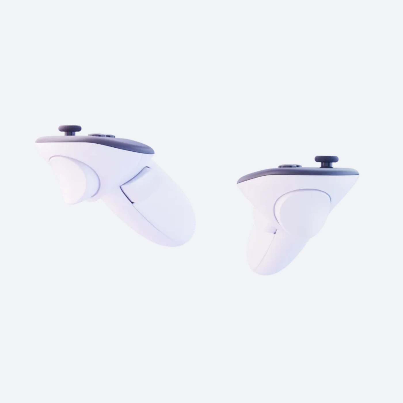
Gamepad Control for Enhanced Operation:
Includes a wireless gamepad for flexible robot control via USB receiver, with open-source demo for custom interaction methods.
Supports 4G/5G Expansion:
Supports installing 4G/5G module* for the application scenarios without Wi-Fi.
Enables Remote Control via Internet:
Our WebRTC-based web demos enable real-time video streaming and remote robot control, with Ngrok tutorials for easy setup.
Supports installing smartphone holder:
Use a spare phone as a hotspot via a holder for low-cost internet-based remote control.
Interactive Tutorials for Hands-on Learning:
Supports Jupyter Lab access on mobile and tablets for easy tutorial reading and code editing online.
Rich Tutorial Resources:
We Provide Complete Tutorials And demos To Help Users Get Started Quickly for Learning and Secondary Development.
₹81395.82
Out of Stock
MRP. ₹125998.60
Incl. GST (No Hidden Charges)