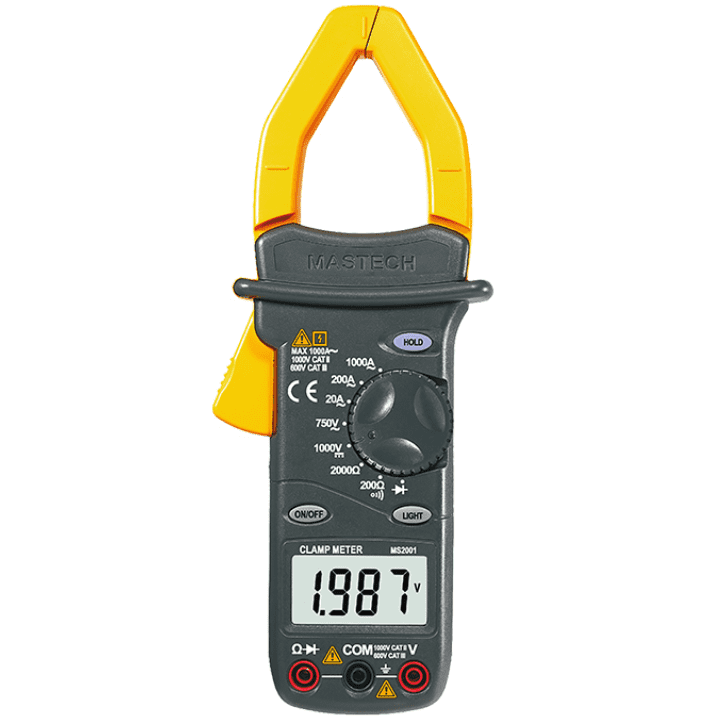
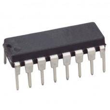
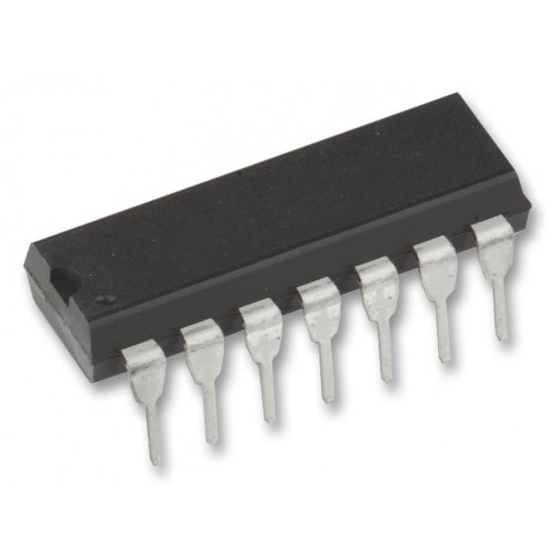
CD4052 - Differential 4-channel Multiplexer/Demultiplexer IC
Delivery & Pickup Options
Order now and we'll have it ready for delivery by the next business day.
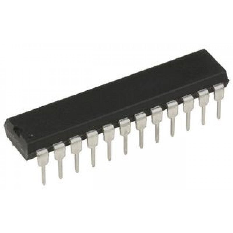
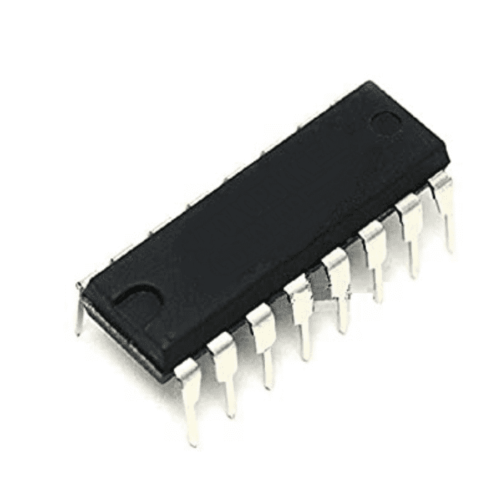
CD4052 - Differential 4-channel Multiplexer/Demultiplexer IC The CD4052 analog multiplexers/demultiplexers IC are digitally controlled analog switches having low “ON” impedance and very low “OFF” leakage currents. Control of analog signals up to 15Vp-p can be achieved by digital signal amplitudes of 3?15V. For example, if VDD = 5V, VSS = 0V and VEE = ?5V, analog signals from ?5V to +5V can be controlled by digital inputs of 0?5V. The multiplexer circuits dissipate extremely low quiescent power over the full VDD?VSS and VDD?VEE supply voltage ranges, independent of the logic state of the control signals. When a logical “1” is present at the inhibit input terminal all channels are “OFF”. CD4052 is a differential 4-channel multiplexer having two binary control inputs, A and B, and an inhibit input. The two binary input signals select 1 or 4 pairs of channels to be turned on and connect the differential analog inputs to the differential outputs. Pinout: Pinout of CD4052 - Differential 4-channel Multiplexer/Demultiplexer IC Pin Number Pin Name Description 16 Vdd Positive power input, maximum 20V 7 Vee Negative power rail, normally connected to ground. 8 Vss (Ground) Connected to ground of the circuit 6 INH Enable pin – Must be pulled to ground for normal operation 9,10 A,B Channel Select pins 1,12 Y0,X0 Channel 0 Input / Output 5,14 Y1,X1 Channel 1 Input / Output 2,15 Y2,X2 Channel 2 Input / Output 4,11 Y3,X3 Channel 3 Input / Output 3,13 Y,X Common Output / Input
- Wide range of digital and analog signal levels
- High “OFF” resistance: channel leakage of ±10 pA (typ.) at VDD − VEE = 10V
- Logic level conversion for digital addressing signals of 3 – 15V (VDD − VSS = 3 – 15V) to switch analog signals to 15 Vp-p (VDD − VEE = 15V)
- Matched switch characteristics: ∆RON = 5Ω (typ.) for VDD − VEE = 15V
- Very low quiescent power dissipation under all digital-control input and supply conditions: 1 µ W (typ.) at VDD − VSS = VDD − VEE = 10V
- Binary address decoding on chip
- Part number CD4052BC
- DC Supply Voltage (VDD) ?0.5 VDC to +18 VDD
- Input Voltage (VIN) ?0.5 VDC to VDD +0.5 VDC
- Storage Temperature Range (TS) ?65°C to +150°C
- Power Dissipation (PD) Dual-In-Line 700 mW
- Lead Temperature (TL) 260°C