

Sort by

14 Stage Ripple Carry Binary …
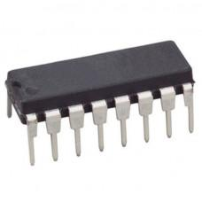
14 Stage Ripple Carry Binary Counter IC - CD4020
The CD4020 IC is a ripple-carry binary counter. All counter stages are master-slave flip-flops. The state of a counter advances one count on the negative transition of each input pulse; a high level on the RESET line resets the counter to its all-zeros state. Schmitt's trigger action on the input-pulse line permits unlimited rise and fall times. All inputs and outputs are buffered.
The CD4x Series CD4020 type is supplied in 16-lead hermetic dual-in-line ceramic packages (F3A suffix), 16-lead dual-in-line plastic packages (E suffix), 16-lead small-outline packages (NSR suffix), and 16-lead thin shrink small-outline packages (PW and PWR suffixes).
check out : CD4040 - 12-Stage Ripple Carry Binary Counter IC
Pinout:
Pinout of CD4020 IC
Applications:
Control counters
Timers
Frequency dividers
Time-delay circuits
Package Includes:
1 x IC - CD4020
Specifications:
Part number
CD4020B
Technology Family
CD4000
VCC (Min) (V)
3
VCC (Max) (V)
18
Bits (#)
12
Voltage (Nom) (V)
5, 10, 15
F @ nom voltage (Max) (MHz)
8
ICC @ nom voltage (Max) (mA)
0.03
tpd @ nom Voltage (Max)(ns)
160
IOL (Max) (mA)
1.5
IOH (Max) (mA)
-1.5
Function
Counter
Type
Binary
Rating
See Data Sheet
Operating temperature range (C)
-55 to 125
Package Group
PDIP|16
₹19.47
₹24.34
Incl. GST

14 Stage Ripple Carry Binary Counter IC - CD4020
14 Stage Ripple Carry Binary Counter IC - CD4020 The CD4020 IC is a ripple-carry binary counter. All counter stages are master-slave flip-flops. The state of a counter advances one …
₹19.47
₹20.63
16-Channel Analog Multiplexer…
16-Channel Analog Multiplexer/Demultiplexer IC - CD4067
CD4067 CMOS analog multiplexers/demultiplexers are digitally controlled analog switches having low ON impedance, low OFF leakage current, and internal address decoding. In addition, the ON resistance is relatively constant over the full input-signal range. The CD4067 is a 16-channel multiplexer with four binary control inputs, A, B, C, D, and an inhibit input, arranged so that any combination of the inputs selects one switch. A logic “1” present at the inhibit input turns all channels off.
The CD4067 type are supplied in 24-lead hermetic dual-in-line ceramic packages (F3A suffix), 24-lead dual-in-line plastic packages (E suffix), 24-lead small-outline packages (M, M96, and NSR suffixes), and 24-lead thin shrink small-outline packages (P and PWR suffixes).
check out : CD4066 - Quad Bilateral Switch IC
Applications:
Analog and digital multiplexing and demultiplexing
A/D and D/A conversion
Signal gating
Package Includes:
Selected qty of IC - CD4067
Specifications:
Part number
CD4067
Configuration
16:01
Number of channels (#)
1
Ron (Typ) (Ohms)
125
Bandwidth (MHz)
14
Rating
Catalog
Operating temperature range (C)
-55 to 125
Package Group
PDIP|24
Input/output continuous current (Max (mA)
10
Supply current (Typ (uA)
0.04
CON (Typ) (pF)
5
₹172.07
₹215.09
Incl. GST

16-Channel Analog Multiplexer/Demultiplexer IC - CD4067
16-Channel Analog Multiplexer/Demultiplexer IC - CD4067 CD4067 CMOS analog multiplexers/demultiplexers are digitally controlled analog switches having low ON impedance, low OFF leakage current, and internal address decoding. In addition, the …
₹172.07
₹182.28
8-bit Up/Down Binary Counter …
8-bit Up/Down Binary Counter IC - CD40193
The CD40193 IC up/down counters are monolithic complementary MOS (CMOS) integrated circuits. The CD40192BM and CD40192BC are BCD counters, while the CD40193BM and CD40193BC are binary counters. Counting up and counting down is performed by two count inputs, one being held high while the other is clocked. The outputs change on the positive-going transition of this clock.
These CD4x Series IC counters feature preset inputs that are enabled when the load is a logical ‘‘0’’ and a clear which forces all outputs to ‘‘0’’ when it is at a logical ‘‘1’’. The counters also have to carry and borrow outputs so that they can be cascaded using no external circuitry. All inputs are protected against damage due to static discharge by clamps to VDD and VSS.
check out : Divide by 8 Counter/Divider IC - CD4022
Pinout:
Pinout of CD40193 IC
Application
Up/Down difference counting
Multistage ripple counting
Synchronous frequency divider
A/D or D/A conversion
BCD counting
Package Includes:
1 x IC - CD40193
Specifications:
Manufacturer's Part Number
CD40193
Category
4000 Series
Package Type
16 Pin DIP
₹59.52
₹74.40
Incl. GST
8-bit Up/Down Binary Counter IC - CD40193
8-bit Up/Down Binary Counter IC - CD40193 The CD40193 IC up/down counters are monolithic complementary MOS (CMOS) integrated circuits. The CD40192BM and CD40192BC are BCD counters, while the CD40193BM and …
₹59.52
₹63.05
CD40106 - Hex Schmitt Trigger…
CD40106 - Hex Schmitt Trigger Inverter IC
The CD40106 IC consists of six Schmitt-Trigger inputs. Each circuit functions as an inverter with Schmitt-Trigger input. The trigger switches at different points for positive- and negative-going signals. The difference between the positive-going voltage (VP) and the negative-going voltage (VN) is defined as hysteresis voltage (VH).
A Schmitt trigger input means that the threshold voltage for going from a HIGH to a LOW input is different from the threshold for going from LOW to HIGH.
CD40106 Pinout Configuration:
Pin Number
Pin Name
Description
1,3,5,11,13,15
Schmitt Input Pins
Input pins of the Schmitt trigger
2,4,6,10,12,14
Schmitt Inverted Output Pins
Output pins of the Schmitt trigger
7
Ground
Connected to the ground of the system
14
Vcc (+5V)
Resets all outputs as low. Must be held high for normal operation
Applications of CD40106:
Noise removing circuits
Debouncing circuits
Hysteresis controller
Dead band filter
Package Includes:
1 x IC - CD40106
Specifications:
Schmitt Trigger
Hex Inverter
Operating Voltage
5V
Low-Level Hysteresis voltage
0.3V
High-Level Hysteresis voltage
3.5V
₹21.64
₹27.06
Incl. GST


CD40106 - Hex Schmitt Trigger Inverter IC
CD40106 - Hex Schmitt Trigger Inverter IC The CD40106 IC consists of six Schmitt-Trigger inputs. Each circuit functions as an inverter with Schmitt-Trigger input. The trigger switches at different points …
₹21.64
₹22.93
CD4011 - Quad 2-Input NAND Ga…
CD4011 - Quad 2-Input NAND Gate IC
The CD4011 is a quad package 2-Input NAND gate IC(Integrated Circuits). That is, it has four NAND gates inside a single package and each gate has two input lines and one output line. All the inputs and outputs are buffered and this improves transfer characteristics by providing a very high gain.
The CD4011 IC operates at 5V, 10V, 15V, and even 20V. When operating at 5V the maximum low-level input voltage is 0.5 and the minimum high-level input voltage is 4.5. All four gates share the same power rail but can operate independently.
Pinout:
Pinout Of CD4011 IC
PACKAGE INCLUDES:
Selected qty of IC - CD4011
Specifications:
Operating Voltage
5V
Low-Level Output Current
1.5mA
Propagation Delay Time
60ns
Operating Temperature Range
- 55 C to + 125 C
₹20.57
₹25.71
Incl. GST


CD4011 - Quad 2-Input NAND Gate IC
CD4011 - Quad 2-Input NAND Gate IC The CD4011 is a quad package 2-Input NAND gate IC(Integrated Circuits). That is, it has four NAND gates inside a single package and …
₹20.57
₹21.79
CD4013 - Dual D Type Flip-Flo…
CD4013 - Dual D Type Flip-Flop IC
The CD4013 designed as a CMOS logic chip IC belongs to the CD4XXX IC series. The CD4013 device comprises two identical, independent data-type flip-flops. Each flip-flop comes with independent data, set, reset, and clock inputs, and Q and Q’ outputs. These devices are commonly used for shift register applications, and, by connecting Q output to the data input, for counter and toggle applications. The logic level present at the D input is transmitted to the Q output during the positive-going transition of the clock pulse. Moreover, the Setting or resetting of IC is independent of the clock and accomplished by a high level on the set or reset line, respectively. The CD4013B is manufactured in 14-pin dual-inline plastic packages (E suffix), 14-pin small-outline packages (M, MT, M96, and NSR suffixes), and 14-pin thin shrink small-outline packages (PW and PWR suffixes).
A D-type Latch/flip-flop is designed as a clocked latch that has two stable states. A D-type latch operates with a delay in input by one clock cycle. Thus, by cascading many D-type flip-flops delay circuits are often created, which are utilized in many applications like in digital television systems. A D-type flip-flop is additionally mentioned as a D flip-flop or a delay flip-flop. The D flip-flop is an edge-triggered device that transfers input files to Q on a clock rising or falling edge. Data Latches are level sensitive devices like the data latch and therefore the transparent latch.
Applications
Power Delivery
Grid Infrastructure
Medical, Healthcare, and Fitness
Body Electronics and Lighting
Building Automation
Telecom Infrastructure
Test and Measurement
Package Includes:
Selected qty of IC - CD4013
Specifications:
Supply Voltage
3 to 20V
Input Current
± 10 mA
Power Dissipation
200mW
Low-level Output Voltage
0.05V
High-level Output Voltage min
4.95V
Low-level Input Voltage Max
1.5V
High-level Input Voltage Min
3.5V
₹15.15
₹18.94
Incl. GST

CD4013 - Dual D Type Flip-Flop IC
CD4013 - Dual D Type Flip-Flop IC The CD4013 designed as a CMOS logic chip IC belongs to the CD4XXX IC series. The CD4013 device comprises two identical, independent data-type …
₹15.15
₹16.05
CD4015 - Dual 4-Stage Shift R…
CD4015 - Dual 4-Stage Shift Register IC
The CD4015 IC consists of two identical, independent, 4-stage serial-input/parallel-output registers. Each register has independent CLOCK and RESET inputs as well as a single serial DATA input. “Q” outputs are available from each of the four stages on both registers. All register stages are D-type, master-slave flip-flops. The logic level present at the DATA input is transferred into the first register stage and shifted over one stage at each positive-going clock transition. Resetting of all stages is accomplished by a high level on the reset line. Register expansion to 8 stages using one CD4015 package, or to more than 8 stages using additional CD4015’s is possible.
The CD4015-series types are supplied in 16-lead hermetic dual-in-line ceramic packages (F3A suffix), 16-lead dual-in-line plastic package (E suffix), 16-lead small-outline packages (M, M96, MT, and NSR suffixes), and 16-lead thin shrink small-outline packages (PW and PWR suffixes).
check out : CD4034 - 8-Stage Bidirectional Bus Register IC (Original)
Pinout:
Pinout Of CD4015 - Dual 4-Stage Shift Register IC
Pin Name
Pin #
Type
Description
VDD
16
Power
Supply Voltage (+3 to +15V)
GND
8
Power
Ground (0V)
DA
7
Input
Data pin for register A
CLKA
9
Input
Clock pulse for register A
RSTA
6
Input
Reset pin for register A
QA0,QA1,QA2,QA3
5,4,3,10
Output
4-bit output for register A
DB
15
Input
Data pin for register B
CLKB
1
Input
Clock pulse for register B
RSTB
14
Input
Reset pin for register B
QB0,QB1,QB2,QB3
11,12,13, 2
Output
4-bit output for register B
Applications:
Serial-input/parallel-output data queueing
Serial to parallel data conversion
General-purpose register
Package Includes:
1 x IC - CD4015
Specifications:
Part number
CD4015B
Technology Family
CD4000
VCC (Min) (V)
3
VCC (Max) (V)
18
Voltage (Nom) (V)
10
F @ nom voltage (Max) (MHz)
8
ICC @ nom voltage (Max) (mA)
0.3
tpd @ nom Voltage (Max (ns)
160
IOL (Max) (mA)
1.5
IOH (Max) (mA)
-1.5
3-state output
No
Operating temperature range (C)
-55 to 125
₹22.73
₹28.40
Incl. GST

CD4015 - Dual 4-Stage Shift Register IC
CD4015 - Dual 4-Stage Shift Register IC The CD4015 IC consists of two identical, independent, 4-stage serial-input/parallel-output registers. Each register has independent CLOCK and RESET inputs as well as a …
₹22.73
₹24.07
CD4016 - Quad Bilateral Switc…
CD4016 - Quad Bilateral Switch IC
The CD4x Series CD4016 is a quad bilateral switch intended for the transmission or multiplexing of analog or digital signals. It is pin-for-pin compatible with CD4066B.
The CD4016 is a CMOS IC with four analog switches, which can be controlled individually using a control pin. The signal can flow in either direction between the two pins of each switch.
Each switch has an enable pin (A) and two input/output pins (X and Y). When the enable pin is set to HIGH, current can flow between X and Y in either direction. However, when enable is LOW, no current can flow between the pins. Just like a switch.
Pinout:
Pinout of CD4016 IC
Pin Name
Pin #
Type
Description
VDD
14
Power
Supply Voltage (+3 to +15V)
GND
7
Power
Ground (0V)
A1-A4
5,6,12,13
Input
Enable pins for the four bilateral switches
X1-X4
1,3,9,11
Input/Output
Pin X for each switch
Y1-Y4
2,4,8,10
Input/Output
Pin Y for each switch
Package Includes:
Selected qty of IC - CD4016
Specifications:
VDD Supply Voltage
−0.5V to +18V
VIN Input Voltage
−0.5V to VDD + 0.5V
TS Storage Temperature Range
−65°C to + 150°C
Power Dissipation (PD): Dual-In-Line
700 mW
Lead Temperature
260°C
₹21.64
₹27.06
Incl. GST

CD4016 - Quad Bilateral Switch IC
CD4016 - Quad Bilateral Switch IC The CD4x Series CD4016 is a quad bilateral switch intended for the transmission or multiplexing of analog or digital signals. It is pin-for-pin compatible …
₹21.64
₹22.93
CD4017 - Decade Counter IC
CD4017 - Decade Counter IC
The CD4017 IC is a decade counter that counts to ten. It has 10 outputs that represent the numbers 0 to 9. The counter increases with one for every rising clock pulse. After the counter has reached 9, it starts again from 0 with the next clock pulse.
This is a great chip for making running LEDs! See a circuit example further down.
check out : Dual Complementary Pair with Inverter IC - CD4007
Pin Overview:
Pinout of CD4017 - Decade Counter IC
Pin Name
Pin #
Type
Description
VDD
16
Power
Supply Voltage (+3 to +15V)
GND
8
Power
Ground (0V)
Q0-Q9
1-7 and 9-11
Output
Qx is high when the counter is x
CO
12
Output
Carry Out. Goes high after ten clock pulses
CI
13
Input
Clock Inhibit. Ignores clock inputs
CLK
14
Input
Clock Input. Increases the counter with one
MR
15
Input
Resets the counter to 0
Package Includes:
Selected qty of IC - CD4017
Specifications:
Input Voltage (VIN)
−0.5 VDC to VDD +0.5 VDC
Storage Temperature (TS)
−65°C to +150°C
DC Supply Voltage (VDD)
−0.5 VDC to +18 VDC
Power Dissipation (PD): Dual-In-Line
700 mW
Lead Temperature (TL)
260°C
₹12.99
₹16.24
Incl. GST


CD4017 - Decade Counter IC
CD4017 - Decade Counter IC The CD4017 IC is a decade counter that counts to ten. It has 10 outputs that represent the numbers 0 to 9. The counter increases …
₹12.99
₹13.76
CD4028 - BCD to Decimal Decod…
CD4028 - BCD to Decimal Decoder IC
CD4028 IC is a BCD to decimal or binary to octal decoder consisting of 4 inputs and 10 output buffers. A BCD code is applied to the 4 inputs, A, B, C, and D. Thus resulting in a high level at the selected 1-of-10 decimal decoded outputs. Similarly, a 3-bit binary code applied to inputs A, B, and C is decoded into octal at outputs 0–7. A high-level signal at the D input inhibits octal decoding and causes outputs 0–7 to go LOW.
The IC is always available in a 16–pin hermetically sealed dual inline IC package (DIP), making it easy to interface with TTL, CMOS, and NMOS devices. The IC offers many features such as high noise immunity and low thermal dissipation. High drive capability is provided at all outputs to enhance dc and dynamic performance in high fan- ut applications. Meanwhile, all the inputs are protected against static discharge damage by diode clamps to VDD and VSS.
A BCD to Decimal Decoder is defined as a simple logic circuit that can translate a BCD (binary coded decimal) input into a decimal (0 – 9) output In any BCD to decimal decoder, the inverters are connected in pairs to make BCD input data available for decoding by the NAND gates. Full decoding of valid BCD input logic ensures that all outputs remain OFF for all invalid binary input conditions. Moreover, these decoders feature TTL inputs and high–performance NPN output transistors designed for use as indicator/relay drivers or as open–collector logic circuit drivers.
check out : CD4514 - 4 Bit Latch/4-16 Line Decoder IC
Pinout:
Pinout of CD4028 IC
Application
Code conversion
Address decoding
Indicator-tube decoder
Package Includes:
Selected qty of IC - CD4028
Specifications:
Supply Voltage Range
3 to 20V
Input or Output Current
±10mA
Power Dissipation
500mW
Low-level Output Voltage Max
0.05V
High-level Output Voltage Min
4.95V
Low-level Input Voltage
2.25V
High-level Input Voltage
2.75V
Propagation Delay Time Max
600ns
Package
DIP-16
₹20.57
₹25.71
Incl. GST

CD4028 - BCD to Decimal Decoder IC
CD4028 - BCD to Decimal Decoder IC CD4028 IC is a BCD to decimal or binary to octal decoder consisting of 4 inputs and 10 output buffers. A BCD code …
₹20.57
₹21.79
