

Sort by

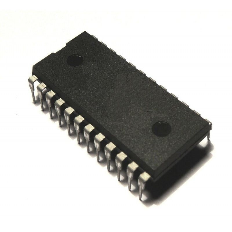
CD4059 - Programmable Divide-…
CD4059 - Programmable Divide-by-N Counter IC
The
CD4x Series
CD4059 standard "A" Series types are divide-by-N down-counters that can be programmed to divide an input frequency by any number "N" from 3 to 15,999. The output signal is a pulse one clock-cycle wide occurring at a rate equal to the input frequency divided by N. This single output has TTL drive capability. The down-counter is preset by means of 16 jam inputs.
The three Mode-Select Inputs Ka, Kb, and Kc determine the modulus ("divide-by" number) of the first and last counting sections. Every time the first (fastest) counting section goes through one cycle, it reduces by 1 the number that has been preset (jammed) into the three decades of the intermediate counting section and into the last counting section, which consists of flip-flops that are not needed for operating the first counting section.
For example, in the 2 modes, only one flip-flop is needed in the first counting section. Therefore the last counting section has three flip-flops that can be preset to a maximum count of seven with a place value of thousands. If 10 is desired for the first section, Ka is set to 1, Kb to 1, and Kc to 0. Jam Inputs J1, J2, J3, and J4 are used to preset the first counting section and there is no last counting section. The intermediate counting section consists of three cascaded BCD decade (10) counters presettable by means of Jam Inputs J5 through J16.
This device is particularly advantageous in communication digital frequency synthesis (VHF, UHF, FM, AM, etc.) where programmable divide-by-"N" counters are an integral part of the synthesizer phase-locked-loop sub-system. The CD4059 can also be used to perform the synthesizer "Fixed Divide-by-R" counting function. It is also useful in general-purpose counters for instrumentation functions such as totalizers, production counters, and "time-out" timers.
The CD4059B-series types are supplied in 24-lead dual-in-line plastic packages (E suffix), and 24-lead small-outline packages (M and M96 suffixes).
Pinout:
Pinout of CD4059 IC
Applications:
Communications digital frequency synthesizers: VHF, UHF, FM, AM, etc.
Fixed or programmable frequency division
"Time out" timer for consumer-application industrial controls
Companion Application Note, ICAN-6374, "Application of the CMOS CD4059A Programmable Divide-by-N Counter in FM and Citizens Band Transceiver Digital Tuners"
₹164.59
MRP. ₹330.40
Incl. GST (No Hidden Charges)
Incl. GST (No Hidden Charges)
CD4059 - Programmable Divide-by-N Counter IC
CD4059 - Programmable Divide-by-N Counter IC The CD4x Series CD4059 standard "A" Series types are divide-by-N down-counters that can be programmed to divide an input frequency by any number "N" …
As low as
₹164.59
₹164.59
MRP. ₹330.40
Incl. GST (No Hidden Charges)
CD4060 - 14 stage Ripple Carr…
CD4060 - 14 stage Ripple Carry Binary Counter IC
The
CD4x Series
CD4060 IC consists of an oscillator section and 14 ripple-carry binary counter stages. The oscillator configuration allows the design of either RC or crystal oscillator circuits. A RESET input is provided which resets the counter to the all-O's state and disables the oscillator. A high level on the RESET line accomplishes the reset function. All counter stages are master-slave flip-flops. The state of the counter is advanced one step in binary order on the negative transition. All inputs and outputs are fully buffered. Schmitt trigger action on the input-pulse line permits unlimited input-pulse rise and fall times.
The CD4060-series types are supplied in 16-lead hermetic dual-in-line ceramic packages (F3A suffix), 16-lead dual-in-line plastic packages (E suffix), 16-lead small-outline packages (M, M96, MT and NSR suffixes), and 16-lead thin shrink small-outline packages (PW and PWR suffixes).
check out :
CD4015 - Dual 4-Stage Shift Register IC
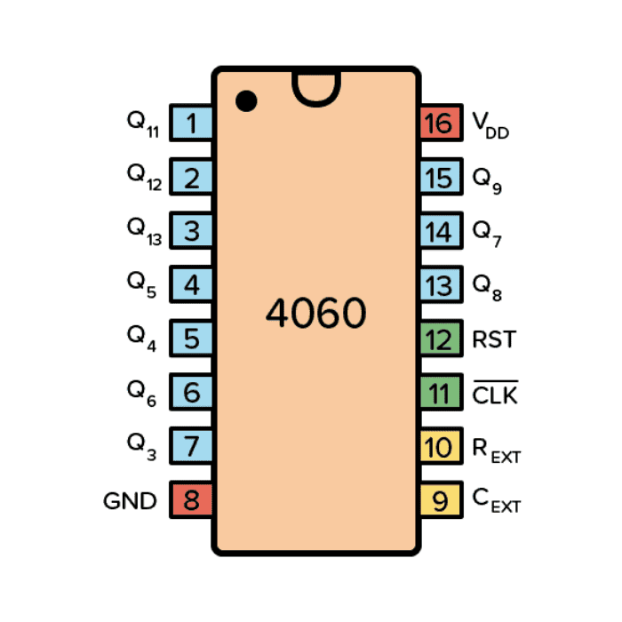
Pinout:
Pinout of CD4060 IC
Pin Name
Pin #
Type
Description
VDD
16
Power
Supply Voltage (+3 to +15V)
GND
8
Power
Ground (0V)
Q3-Q9
1-7
Output
Counter outputs
Q11-Q13
13-15
Output
Counter outputs
C
EXT
9
Input
Connection for an external capacitor
R
EXT
10
Input
Connection for external resistor
CLK
11
Input
Clock input/Oscillator pin
RST
12
Input
Resets the counter
Applications:
Control counters
Timers
Frequency dividers
Time-delay circuits
check out :
CD4013 - Dual D Type Flip-Flop IC
₹15.25
MRP. ₹26.60
Incl. GST (No Hidden Charges)
Incl. GST (No Hidden Charges)
CD4060 - 14 stage Ripple Carry Binary Counter IC
CD4060 - 14 stage Ripple Carry Binary Counter IC The CD4x Series CD4060 IC consists of an oscillator section and 14 ripple-carry binary counter stages. The oscillator configuration allows the …
As low as
₹15.25
₹15.25
MRP. ₹26.60
Incl. GST (No Hidden Charges)
CD4066 - Quad Bilateral Switc…
CD4066 - Quad Bilateral Switch IC
The CD4066 device is a quad bilateral switch intended for the transmission or multiplexing of analog or digital signals. It is pin-for-pin compatible with the CD4016 device but exhibits a much lower on-state resistance. In addition, the on-state resistance is relatively constant over the full signal-input range.
The
CD4x Series
CD4066 device consists of four bilateral switches, each with independent controls. Both the p and the n devices in a given switch are biased on or off simultaneously by the control signal. The well of the n-channel device on each switch is tied to either the input (when the switch is on) or to V
SS
(when the switch is off). This configuration eliminates the variation of the switch-transistor threshold voltage with the input signal and, thus, keeps the on-state resistance low over the full operating-signal range.
The advantages over single-channel switches include peak input-signal voltage swings equal to the full supply voltage and more constant on-state impedance over the input-signal range. However, for sample-and-hold applications, the CD4016 device is recommended.
check out :
CD4016 - Quad Bilateral Switch IC
Pinout:
Pinout of CD4066 IC
₹16.26
MRP. ₹40.60
Incl. GST (No Hidden Charges)
Incl. GST (No Hidden Charges)

CD4066 - Quad Bilateral Switch IC
CD4066 - Quad Bilateral Switch IC The CD4066 device is a quad bilateral switch intended for the transmission or multiplexing of analog or digital signals. It is pin-for-pin compatible with …
As low as
₹16.26
₹16.26
MRP. ₹40.60
Incl. GST (No Hidden Charges)
CD4069 - Hex Inverter IC
CD4069 - Hex Inverter IC
The CD4069
IC
device consists of six CMOS inverter circuits. These devices are intended for all general-purpose inverter applications where the medium-power TTL drive and logic-level-conversion capabilities of circuits such as the CD4009 and CD4049 hex inverter and buffers are not required.
check out :
CD4049 - Hex Inverting Buffer/Converter IC
Pinout:
Pinout of CD4069 - Hex Inverter IC
₹15.25
MRP. ₹37.80
Incl. GST (No Hidden Charges)
Incl. GST (No Hidden Charges)
CD4069 - Hex Inverter IC
CD4069 - Hex Inverter IC The CD4069 IC device consists of six CMOS inverter circuits. These devices are intended for all general-purpose inverter applications where the medium-power TTL drive and …
As low as
₹15.25
₹15.25
MRP. ₹37.80
Incl. GST (No Hidden Charges)
CD4070 - Quad 2-Input Exclusi…
CD4070 - Quad 2-Input Exclusive-OR (XOR) Gate IC
The CD4070
IC
contains four independent Exclusive OR gates inside a single package. It is oftentimes referred to as a
quad package 2-Input XOR gate IC. All four gates share the same power rail and each gate has two input lines and one output line. This IC gives the system designer a way to directly implement the Exclusive-OR Boolean function. The CD4070 makes use of complementary MOS (CMOS) transistors to achieve a broad power supply operating range, low power consumption, and a high noise margin. The IC operates at 5V, 10V, 15V, and even 20V. When operating at 5V the maximum low-level input voltage is 0.5 and the minimum high-level input voltage is 4.5.
check out :
CD4078 - 8 Input NOR Gate IC
Pinout:
Pinout Of CD4070 IC
Pin Name
Pin #
Type
Description
VDD
14
Power
Supply Voltage (+3 to +15V)
GND
7
Power
Ground (0V)
A1 to A4
1, 5, 8, 12
Input
Inputs A of the four XOR gates
B1 to B4
2, 6, 9, 13
Input
Inputs B of the four XOR gates
Q1 to Q4
3, 4, 10, 11
Output
Outputs from the four XOR gates
₹20.32
MRP. ₹47.60
Incl. GST (No Hidden Charges)
Incl. GST (No Hidden Charges)

CD4070 - Quad 2-Input Exclusive-OR (XOR) Gate IC
CD4070 - Quad 2-Input Exclusive-OR (XOR) Gate IC The CD4070 IC contains four independent Exclusive OR gates inside a single package. It is oftentimes referred to as a quad package …
As low as
₹20.32
₹20.32
MRP. ₹47.60
Incl. GST (No Hidden Charges)
CD4078 - 8 Input NOR Gate IC
CD4078 - 8 Input NOR Gate IC
The CD4078 NOR/OR Gate
IC
provides the system designer with direct implementation of the positive logic 8-input NOR and OR functions and supplements the existing family of CMOS gates.
The CD4078 types are supplied in 14-lead hermetic dual-in-line ceramic packages (F3A suffix), 14-lead dual-in-line plastic packages (E suffix), 14-lead small-outline packages (M, MT, M96, and NSR suffixes), and 14-lead thin shrink small-outline packages (PW and PWR suffixes).
check out :
Quad 2-input OR gate IC - CD4071
Application:
Mixer tank
Memory circuits
File registers
₹32.51
MRP. ₹54.60
Incl. GST (No Hidden Charges)
Incl. GST (No Hidden Charges)

CD4078 - 8 Input NOR Gate IC
CD4078 - 8 Input NOR Gate IC The CD4078 NOR/OR Gate IC provides the system designer with direct implementation of the positive logic 8-input NOR and OR functions and supplements …
As low as
₹32.51
₹32.51
MRP. ₹54.60
Incl. GST (No Hidden Charges)
CD4081 - Quad 2 Input AND Gat…
CD4081 - Quad 2 Input AND Gate IC
CD4081 Quad 2 Input AND gates
IC
provides the system designer with direct implementation of the AND function and supplements the existing family of CMOS gates.
The CD4081 types are supplied in 14-lead hermetic dual-in-line ceramic packages (F3A suffix), 14-lead dual-in-line plastic packages (E suffix), 14-lead small-outline packages (M, MT, M96, and NSR suffixes), and 14-lead thin shrink small-outline packages (PW and PWR suffixes).
check out :
CD4532 - 8 Bit Priority Encoder IC (Original)
Pinout:
Pinout Of CD4081 IC
check out :
CD4030 - Quad 2-Input Exclusive OR (EXOR) Gate IC
₹17.28
MRP. ₹42.00
Incl. GST (No Hidden Charges)
Incl. GST (No Hidden Charges)

CD4081 - Quad 2 Input AND Gate IC
CD4081 - Quad 2 Input AND Gate IC CD4081 Quad 2 Input AND gates IC provides the system designer with direct implementation of the AND function and supplements the existing …
As low as
₹17.28
₹17.28
MRP. ₹42.00
Incl. GST (No Hidden Charges)
CD4093 - Quad 2-Input NAND Sc…
CD4093 - Quad 2-Input NAND Schmitt Trigger IC
CD4093 consists of four Schmitt-trigger circuits. Each circuit functions as a two-input NAND gate with Schmitt-trigger action on both inputs. The gate switches at different points for positive- and negative-going signals. The difference between the positive voltage (V
P
) and the negative voltage (V
N
) is defined as hysteresis voltage (V
H
) (see Fig. 2).
The CD4093 types are supplied in 14-lead hermetic dual-in-line ceramic packages (F3A suffix), 14-lead dual-in-line plastic packages (E suffix), 14-lead small-outline packages (M, MT, M96, and NSR suffixes), and 14-lead thin shrink small-outline packages (PW and PWR suffixes).
check out :
Dual 4-Input OR Gate IC - CD4072
Pinout:
Pinout of CD4093 - Quad 2-Input NAND Schmitt Trigger IC
Pin Name
Pin #
Type
Description
VDD
14
Power
Supply Voltage (+3 to +15V)
GND
7
Power
Ground (0V)
A1 to A4
1, 5, 8, 12
Input
Inputs A of the four NAND gates
B1 to B4
2, 6, 9, 13
Input
Inputs B of the four NAND gates
Q1 to Q4
3, 4, 10, 11
Output
Outputs from the four NAND gates
Applications:
Wave and pulse shapers
High-noise-environment systems
Monostable multivibrators
Astable multivibrators
NAND logic
₹20.32
MRP. ₹47.60
Incl. GST (No Hidden Charges)
Incl. GST (No Hidden Charges)

CD4093 - Quad 2-Input NAND Schmitt Trigger IC
CD4093 - Quad 2-Input NAND Schmitt Trigger IC CD4093 consists of four Schmitt-trigger circuits. Each circuit functions as a two-input NAND gate with Schmitt-trigger action on both inputs. The gate …
As low as
₹20.32
₹20.32
MRP. ₹47.60
Incl. GST (No Hidden Charges)
CD4094 - 8-Stage Shift and St…
CD4094 - 8-Stage Shift and Store Bus Register IC
The CD4094
IC
belongs to the CD4000 IC series. This IC is composed of an 8-bit shift register and a 3- State 8-bit latch. In this IC, Data shifted serially through the shift register on the positive transition of the clock. The CD4082 IC operates at a wide range of working voltage, a wide range of working conditions. And directly interfaces with CMOS, NMOS, and TTL. The output of the IC always comes in TTL which makes it quite easy to function with other TTL devices and microcontrollers.
CD4094 offers features such as ESD barring and high noise immunity. Each output is protected against static damage by using clamping diodes. CD4094 Operates at a supply voltage of range between 3V to 20V. This IC is designed for operation over the full military temperature range of 0°C to 70°C. The IC CD4094 comes as smaller in size and offers much faster speed which makes it highly reliable in every kind of device. CD4094 IC can be soldered directly to the circuit board or easily mounted on a 16 pin IC base.
Shift-and-Store Bus Register is designed as a digital memory circuitry available in devices such as calculators, computers, and data processing systems. Using a Shift-and-Store Bus Register, data or bits enter into the system in a serial or parallel manner. Data entry is performed from one direction, and as more data is added, it shifts positions until the data gets to the output end. The two ends are referred to as the left and right ends. Whereas the movement of data occurs from left to right, from right to left. Or in both directions to make a bidirectional register.
check out :
CD4099 - 8 bit Addressable Latch IC
Pinout:
Pinout of CD4094 - 8-Stage Shift and Store Bus Register IC
Applications:
Serial-to-Parallel data conversion
Remote control holding register
Dual rank shift, hold, and bus register
₹22.35
MRP. ₹47.60
Incl. GST (No Hidden Charges)
Incl. GST (No Hidden Charges)

CD4094 - 8-Stage Shift and Store Bus Register IC
CD4094 - 8-Stage Shift and Store Bus Register IC The CD4094 IC belongs to the CD4000 IC series. This IC is composed of an 8-bit shift register and a 3- …
As low as
₹22.35
₹22.35
MRP. ₹47.60
Incl. GST (No Hidden Charges)
CD4099 - 8 bit Addressable La…
CD4099 - 8 bit Addressable Latch IC
The CD4099 8-bit addressable latch
IC
is a serial-input, parallel-output storage register that can perform a variety of functions. Data are inputted to a particular bit in the latch when that bit is addressed (by means of input A0, A1, A2) and when WRITE DISABLE is at a low level. When WRITE DISABLE is high, data entry is inhibited; however, all 8 outputs can be continuously read independently of WRITE DISABLE and address inputs.
A master RESET input is available, which resets all bits to a logic "0" level when RESET and WRITE DISABLE is at a high level. When RESET is at a high level, and WRITE RESET is at a low level, the latch acts as a 1-of-8 demultiplexer; the bit that is addressed has an active output that follows the data input, while all unaddressed bits are held to a logic "0" level.
The CD4099 types are supplied in 16-lead hermetic dual-in-line ceramic packages (F3A suffix), 16-lead dual-in-line plastic packages (E suffix), 16-lead small-outline packages (M, M96, MT, and NSR suffixes), and 16-lead thin shrink small-outline packages (PW and PWR suffixes).
check out :
Quad NOR R-S Latch Tri-state IC - CD4043
Pinout:
Pin No
Pin Name
Description
1
Q7
Output Pin 7 of Latch
2
CL
Clear Output Pin
3
D
Data Input
4
E’
Enable Pin
5
A0
Input Pin 0 of Latch
6
A1
Input Pin 1 of Latch
7
A2
Input Pin 2 of Latch
8
VSS
Source Supply
9
Q0
Output Pin 0 of Latch
10
Q1
Output Pin 1 of Latch
11
Q2
Output Pin 2 of Latch
12
Q3
Output Pin 3 of Latch
13
Q4
Output Pin 4 of Latch
14
Q5
Output Pin 5 of Latch
15
Q6
Output Pin 6 of Latch
16
VDD
Drain Supply
Applications:
Multi-line decoders
A/D converters
₹26.42
MRP. ₹49.00
Incl. GST (No Hidden Charges)
Incl. GST (No Hidden Charges)

CD4099 - 8 bit Addressable Latch IC
CD4099 - 8 bit Addressable Latch IC The CD4099 8-bit addressable latch IC is a serial-input, parallel-output storage register that can perform a variety of functions. Data are inputted to …
As low as
₹26.42
₹26.42
MRP. ₹49.00
Incl. GST (No Hidden Charges)
