

Sort by

CD4504 - Hex Voltage Level Sh…
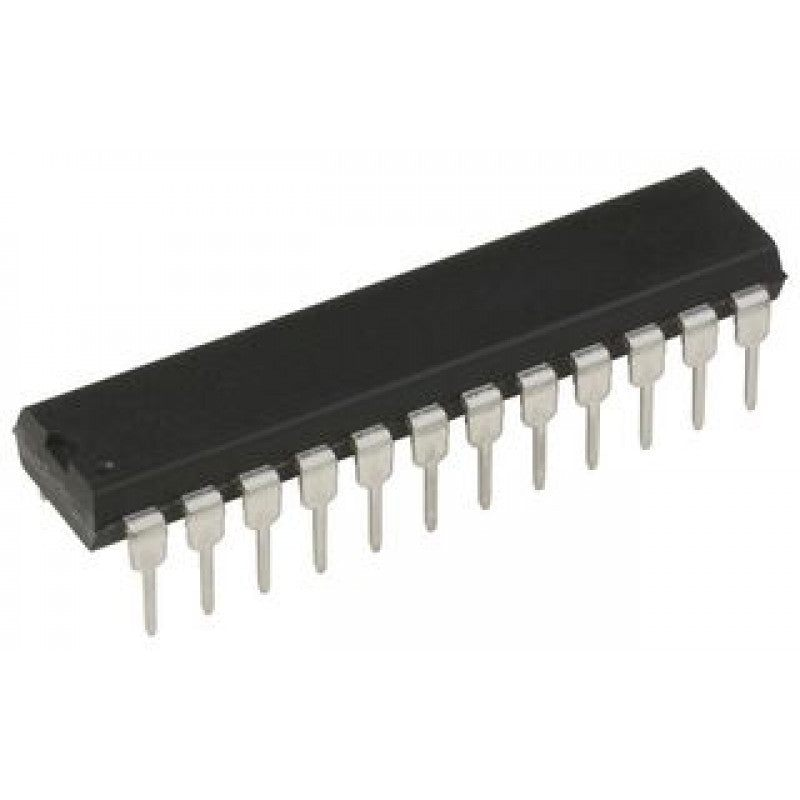
CD4504 - Hex Voltage-Level Shifter IC
The CD4504 hex voltage level shifter
IC
consists of six circuits that shift input signals from the V
CC
logic level to the V
DD
logic level. To shift TTL signals to CMOS logic levels, the SELECT input is at the V
CC
HIGH logic state. When the SELECT input is in a LOW logic state, each circuit translates signals from one CMOS level to another.
The CD4504 types are supplied in 16-lead hermetic dual-in-line ceramic packages (F3A suffix), 16-lead dual-in-line plastic packages (E suffix), 16-lead small-outline packages (M, M96, and MT suffixes), and 16-lead thin shrink small-outline packages (PW and PWR suffixes).
Pinout:
Pin No
Pin Name
Description
1
VCC
Collector supply voltage
2
AOUT
output of level shifter A
3
AIN
input of level shifter A
4
BOUT
output of level shifter B
5
BIN
input of level shifter B
6
COUT
output of level shifter C
7
CIN
input of level shifter C
8
VSS
source supply
9
DIN
input of level shifter D
10
DOUT
output of level shifter D
11
EIN
input of level shifter E
12
EOUT
output of level shifter E
13
SELECT
select pin
14
FIN
input of level shifter F
15
FOUT
output of level shifter F
16
VDD
Drain supply
₹28.45
MRP. ₹49.00
Incl. GST (No Hidden Charges)
Incl. GST (No Hidden Charges)

CD4504 - Hex Voltage Level Shifter IC
CD4504 - Hex Voltage-Level Shifter IC The CD4504 hex voltage level shifter IC consists of six circuits that shift input signals from the V CC logic level to the V …
As low as
₹28.45
₹28.45
MRP. ₹49.00
Incl. GST (No Hidden Charges)
CD4511 - BCD To 7 Segment Lat…
CD4511 - BCD To 7 Segment Latch Decoder Driver IC
The CD4511 IC types are BCD-to-7-segment latch decoder drivers constructed with CMOS logic and n-p-n bipolar transistor output devices on a single monolithic structure. These devices combine the low quiescent power dissipation and high noise immunity features of RCA CMOS with n-p-n bipolar output transistors capable of sourcing up to 25 MA. This capability allows the CD4511 types to drive LED's and other displays directly.
Lamp Test (LT)\, Blanking (BL)\, and Latch Enable or Strobe inputs are provided to test the display, shut off or intensity-modulated it, and store or strobe a BCD code, respectively. Several different signals may be multiplexed and displayed when external multiplexing circuitry is used.
The
CD4x Series
CD4511 types are supplied in 16-lead hermetic dual-in-line ceramic packages (F3A suffix), 16-lead dual-in-line plastic packages (E suffix), 16-lead small-outline packages (NSR suffix), and 16-lead thin shrink small-outline packages (PW and PWR suffixes).
These devices are similar to the type MC14511.
check out :
CD4543 - BCD to 7 Segment Decoder IC
Pinout:
Pinout of CD4511 IC
Pin Name
Pin #
Type
Description
VDD
16
Power
Supply Voltage (+3 to +15V)
GND
8
Power
Ground (0V)
a-f
9-15
Output
Outputs for the 7-segment display
D0-D3
7, 1, 2, 6
Input
4-bit data input
LT
3
Input
Lamp Test. Turns on all segments when LOW.
BL
4
Input
Blanking Test. Turns off all segments when LOW.
LE
5
Input
Latch Enable. Stores the current state when HIGH
Applications:
Driving common-cathode LED displays
Multiplexing with common-cathode LED displays
Driving incandescent displays
Driving low-voltage fluorescent displays
₹16.26
MRP. ₹54.60
Incl. GST (No Hidden Charges)
Incl. GST (No Hidden Charges)

CD4511 - BCD To 7 Segment Latch Decoder Driver IC
CD4511 - BCD To 7 Segment Latch Decoder Driver IC The CD4511 IC types are BCD-to-7-segment latch decoder drivers constructed with CMOS logic and n-p-n bipolar transistor output devices on …
As low as
₹16.26
₹16.26
MRP. ₹54.60
Incl. GST (No Hidden Charges)
CD4514 - 4 Bit Latch/4-16 Lin…
CD4514 - 4 Bit Latch/4-16 Line Decoder IC
The
CD4x Series
CD4514 IC is a 4-to-16-line decoder with latched inputs implemented with complementary MOS (CMOS) circuits constructed with N- and P-channel enhancement mode transistors. These circuits are primarily used in decoding applications where low power dissipation and/or high noise immunity are required.
The CD4514 (output active high option) presents a logical “1” at the selected output. The input latches are R–S type flip-flops, which hold the last input data presented prior to the strobe transition from “1” to “0”. This input data is decoded and the corresponding output is activated. An output inhibits line is also available.
Pinout:
Pinout Of CD4514 IC
₹166.62
MRP. ₹278.60
Incl. GST (No Hidden Charges)
Incl. GST (No Hidden Charges)
CD4514 - 4 Bit Latch/4-16 Line Decoder IC
CD4514 - 4 Bit Latch/4-16 Line Decoder IC The CD4x Series CD4514 IC is a 4-to-16-line decoder with latched inputs implemented with complementary MOS (CMOS) circuits constructed with N- and …
As low as
₹166.62
₹166.62
MRP. ₹278.60
Incl. GST (No Hidden Charges)
CD4518 - Dual BCD Up Counter …
CD4518 - Dual BCD Up Counter IC
The
CD4x Series
CD4518 consists of two identical, internally synchronous 4-stage counters. The counter stages are D-type flip-flops having interchangeable CLOCK and ENABLE lines for incrementing on either the positive-going or negative-going transition. For single-unit operation, the ENABLE input is maintained high and the counter advances on each positive-going transition of the CLOCK.
The counters are cleared by high levels on their RESET lines. The counter can be cascaded in the ripple mode by connecting Q4 to the enable input of the subsequent counter while the CLOCK input of the latter is held low. The CD4518 types are supplied in 16-lead hermetic dual-in-line ceramic packages (F3A suffix), 16-lead dual-in-line plastic packages (E suffix), 16-lead small-outline packages (M, M96, and NSR suffixes), and 16-lead thin shrink small-outline packages (PW and PWR suffixes).
check out :
CD4059 - Programmable Divide-by-N Counter IC
Pinout:
Pinout of CD4518 IC
Applications:
Multistage synchronous counting
Multistage ripple counting
Frequency dividers
₹22.35
MRP. ₹44.80
Incl. GST (No Hidden Charges)
Incl. GST (No Hidden Charges)

CD4518 - Dual BCD Up Counter IC (Original)
CD4518 - Dual BCD Up Counter IC The CD4x Series CD4518 consists of two identical, internally synchronous 4-stage counters. The counter stages are D-type flip-flops having interchangeable CLOCK and ENABLE …
As low as
₹22.35
₹22.35
MRP. ₹44.80
Incl. GST (No Hidden Charges)
CD4519 - Quad AND/OR Select G…
CD4519 - Quad AND/OR Select Gate IC
The
CD4x Series
CD4519 CMOS IC can be configured as 4-bit AND/OR selectors, as quad 2-channel data selectors, or as quad exclusive-NOR gates. This is achieved by setting the control inputs to produce the particular function desired. The
single supply voltage of the CD4519 quad IC is 3V to 18V.
Pinout:
Pinout of CD4519 IC
₹104.64
MRP. ₹208.60
Incl. GST (No Hidden Charges)
Incl. GST (No Hidden Charges)
CD4519 - Quad AND/OR Select Gate IC (Original)
CD4519 - Quad AND/OR Select Gate IC The CD4x Series CD4519 CMOS IC can be configured as 4-bit AND/OR selectors, as quad 2-channel data selectors, or as quad exclusive-NOR gates. …
As low as
₹104.64
₹104.64
MRP. ₹208.60
Incl. GST (No Hidden Charges)
CD4532 - 8 Bit Priority Encod…
CD4532 - 8 Bit Priority Encoder IC
The
CD4x Series
CD4532 consists of combinational logic that encodes the highest priority input (D7-D0) to a 3-bit binary code. The eight inputs, D7 through D0, each have an assigned priority; D7 is the highest priority and D0 is the lowest. The priority encoder is inhibited when the chip-enable input E
I
is low. When E
I
is high, the binary representation of the highest-priority input appears on output lines Q2-Q0, and the group select line GS is high to indicate that priority inputs are present. The enable-out (E
O
) is high when no priority inputs are present. If any one input is high, E
O
is low and all cascaded lower-order stages are disabled.
The CD4532 types are supplied in 16-lead hermetic dual-in-line ceramic packages (F3A suffix), 16-lead dual-in-line plastic packages (E suffix), 16-lead small-outline packages (M, M96, MT, and NSR suffixes), and 16-lead thin shrink small-outline packages (PW and PWR suffixes).
Pinout:
Pinout of CD4532 IC
Applications:
Priority encoder
Binary or BCD encoder (keyboard encoding)
Floating-point arithmetic
₹44.70
MRP. ₹81.20
Incl. GST (No Hidden Charges)
Incl. GST (No Hidden Charges)

CD4532 - 8 Bit Priority Encoder IC (Original)
CD4532 - 8 Bit Priority Encoder IC The CD4x Series CD4532 consists of combinational logic that encodes the highest priority input (D7-D0) to a 3-bit binary code. The eight inputs, …
As low as
₹44.70
₹44.70
MRP. ₹81.20
Incl. GST (No Hidden Charges)
CD4538 - Dual Precision Monos…
CD4538 - Dual Precision Monostable Multivibrator IC
The CD4538
IC
is a dual, precision monostable multivibrator with independent trigger and reset controls. The device is re-triggerable and resettable, and the control inputs are internally latched. Two trigger inputs are provided to allow either rising or falling edge triggering. The reset inputs are active low and prevent triggering while active. Precise control of output pulse-width has been achieved using linear CMOS techniques.
The pulse duration and accuracy are determined by external components RX and CX. The device does not allow the timing capacitor to discharge through the timing pin on power-down conditions. For this reason, no external protection resistor is required in series with the timing pin. Input protection from static discharge is provided on all pins.
Pinout:
Pinout of CD4538 - Dual Precision Monostable Multivibrator IC
₹26.42
MRP. ₹54.60
Incl. GST (No Hidden Charges)
Incl. GST (No Hidden Charges)

CD4538 - Dual Precision Monostable Multivibrator IC
CD4538 - Dual Precision Monostable Multivibrator IC The CD4538 IC is a dual, precision monostable multivibrator with independent trigger and reset controls. The device is re-triggerable and resettable, and the …
As low as
₹26.42
₹26.42
MRP. ₹54.60
Incl. GST (No Hidden Charges)
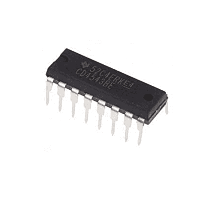
CD4543 - BCD to 7 Segment Dec…
CD4543 - BCD to 7 Segment Decoder IC
The CD4543
IC
is a BCD-to-seven segment latch/decoder/driver IC designed primarily for liquid-crystal display (LCD) applications. It is also capable of driving light-emitting diode (LED), incandescent, gas-discharge, and fluorescent displays. This device is functionally similar and serves as a direct replacement for the CD4056 when pin 7 is connected to VSS. It differs from the CD4056B in that it has a display blanking capability instead of a level-shifting function and requires only one power supply.
When the CD4056 is used in the level shifting mode, two power supplies are required. When the CD4543 is used for LCD applications, a square wave must be applied to the PHASE input and the backplane of the LCD device. For LED applications logic 1 is required at the PHASE input for common-cathode devices; logic 0 is required for common-anode devices (see truth table). The CD4543B is supplied in 16-lead dual-in-line plastic packages (E suffix), 16-lead small-outline packages (M, M96, MT, and NSR suffixes), and 16-lead thin shrink small-outline packages (PW and PWR suffixes).
Pinout:
Pinout of CD4543 - BCD to 7 Segment Decoder IC
Applications:
Instrument display driver
Dashboard display driver
Computer/calculator display driver
Timing device driver (clocks, watches, timers)
₹38.61
MRP. ₹61.60
Incl. GST (No Hidden Charges)
Incl. GST (No Hidden Charges)

CD4543 - BCD to 7 Segment Decoder IC
CD4543 - BCD to 7 Segment Decoder IC The CD4543 IC is a BCD-to-seven segment latch/decoder/driver IC designed primarily for liquid-crystal display (LCD) applications. It is also capable of driving …
As low as
₹38.61
₹38.61
MRP. ₹61.60
Incl. GST (No Hidden Charges)
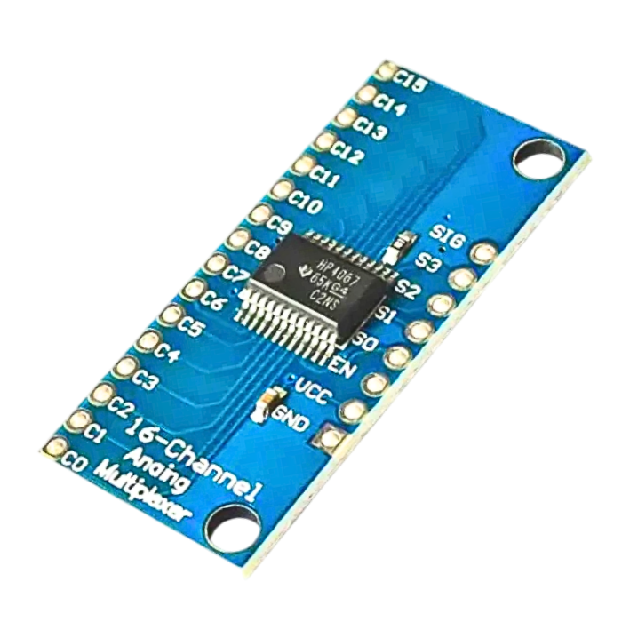
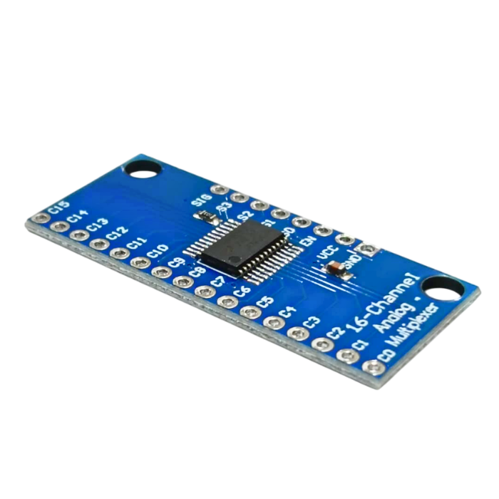
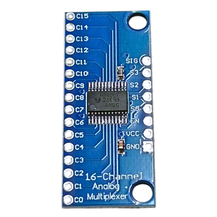
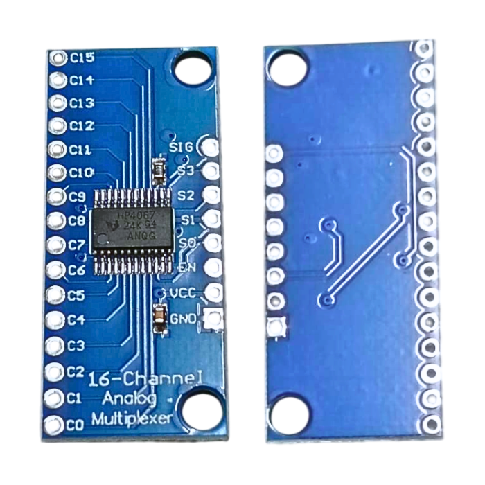
CD74HC4067 16 Channel Analog …
CD74HC4067 16 Channel Analog Multiplexer Breakout Module
The CD74HC4067 16-Channel Analog Multiplexer Breakout Module is a powerful and efficient breakout board and best solution for expanding input and output options in electronics projects. Acting like a rotary switch, it allows a single common pin (SIG) to connect to one of 16 channels (CHANxx), enabling seamless integration of multiple sensors or signals with minimal wiring.
This 16 channel analog multiplexer module simplifies circuit design by reducing the number of required microcontroller pins to just five control lines (S0–S3 and EN). This makes it perfect for microcontrollers with limited I/O while maintaining reliable, high-speed switching.
Designed for versatility, the CD74HC4067 (High-speed CMOS) supports bidirectional signal flow and operates with voltages up to VCC. Its low on-resistance and minimal leakage current ensure accurate signal transmission without interference.
The break-before-make switching prevents crosstalk, making this CD4067 multiplexer module an ideal for sensor arrays, data acquisition systems, and serial communication multiplexing. Additionally, the 16 channel breakout module features an enable pin, allowing all connections to be disabled when not in use.
For expanding sensor inputs, managing multiple communication lines, and optimizing circuit efficiency, this Multiplexer breakout board provides a compact, reliable, and cost-effective solution for a wide range of applications.
Features
Operates within a voltage range of 2V to 6V for flexible integration.
On resistance of just 70 Ohms at 4.5V, ensuring minimal signal loss.
Fast 6ns break-before-make switching for precise and quick signal routing.
Wide operating temperature range of -55°C to 125°C, suitable for harsh environments.
Ensures reliable performance even in extreme conditions.
Ideal for applications requiring high-speed switching and temperature tolerance.
₹49.78
MRP. ₹103.60
Incl. GST (No Hidden Charges)
Incl. GST (No Hidden Charges)


CD74HC4067 16 Channel Analog Multiplexer Breakout Module
CD74HC4067 16 Channel Analog Multiplexer Breakout Module The CD74HC4067 16-Channel Analog Multiplexer Breakout Module is a powerful and efficient breakout board and best solution for expanding input and output options …
As low as
₹49.78
₹49.78
MRP. ₹103.60
Incl. GST (No Hidden Charges)
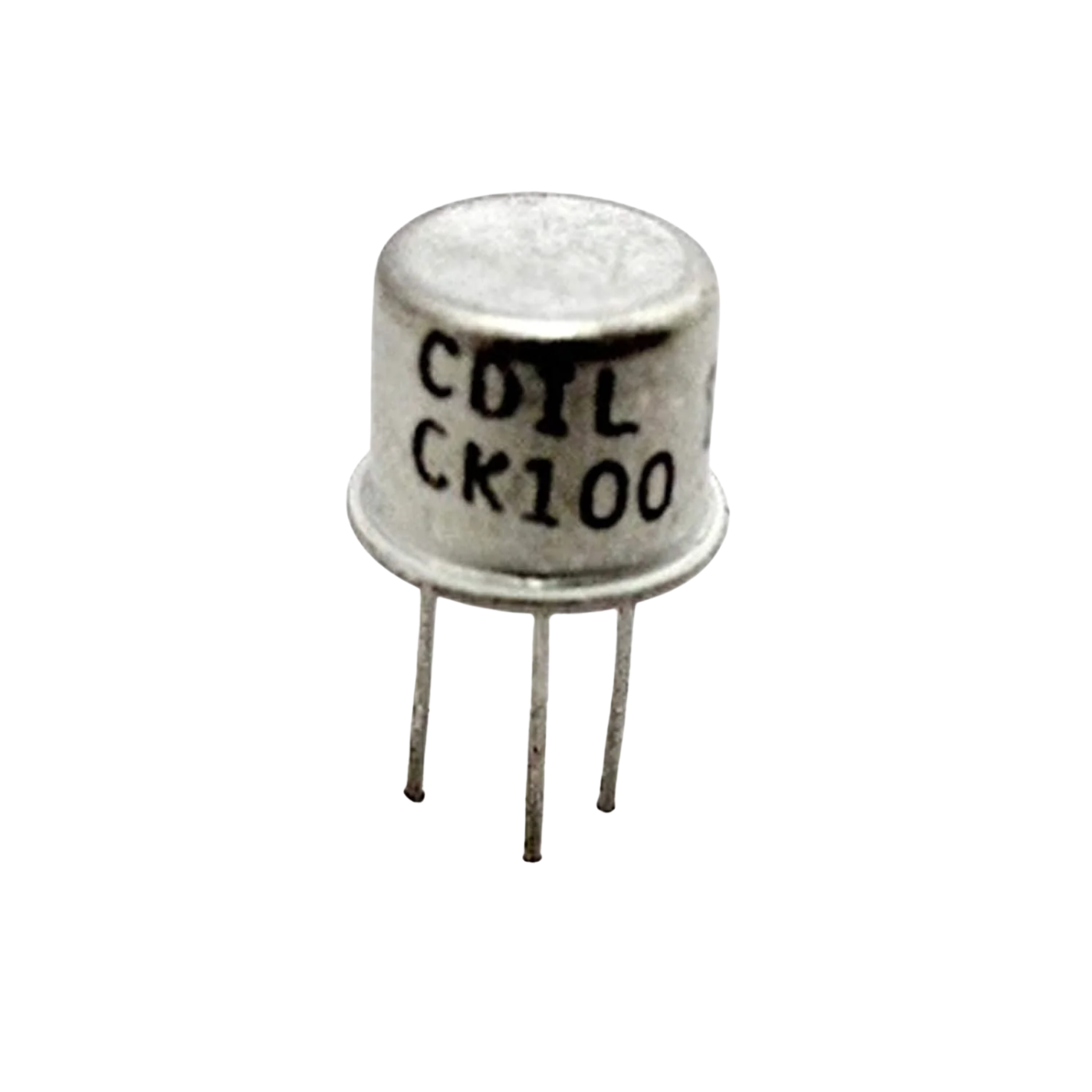
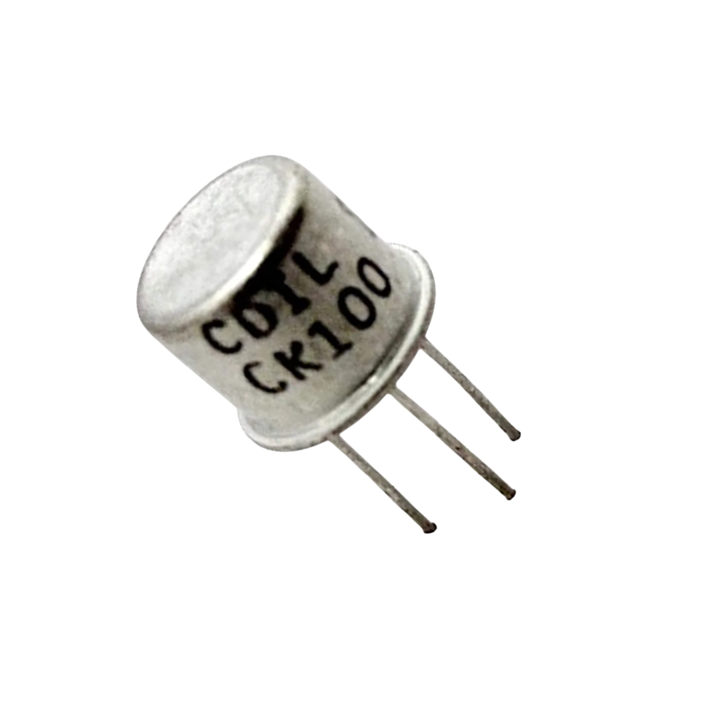
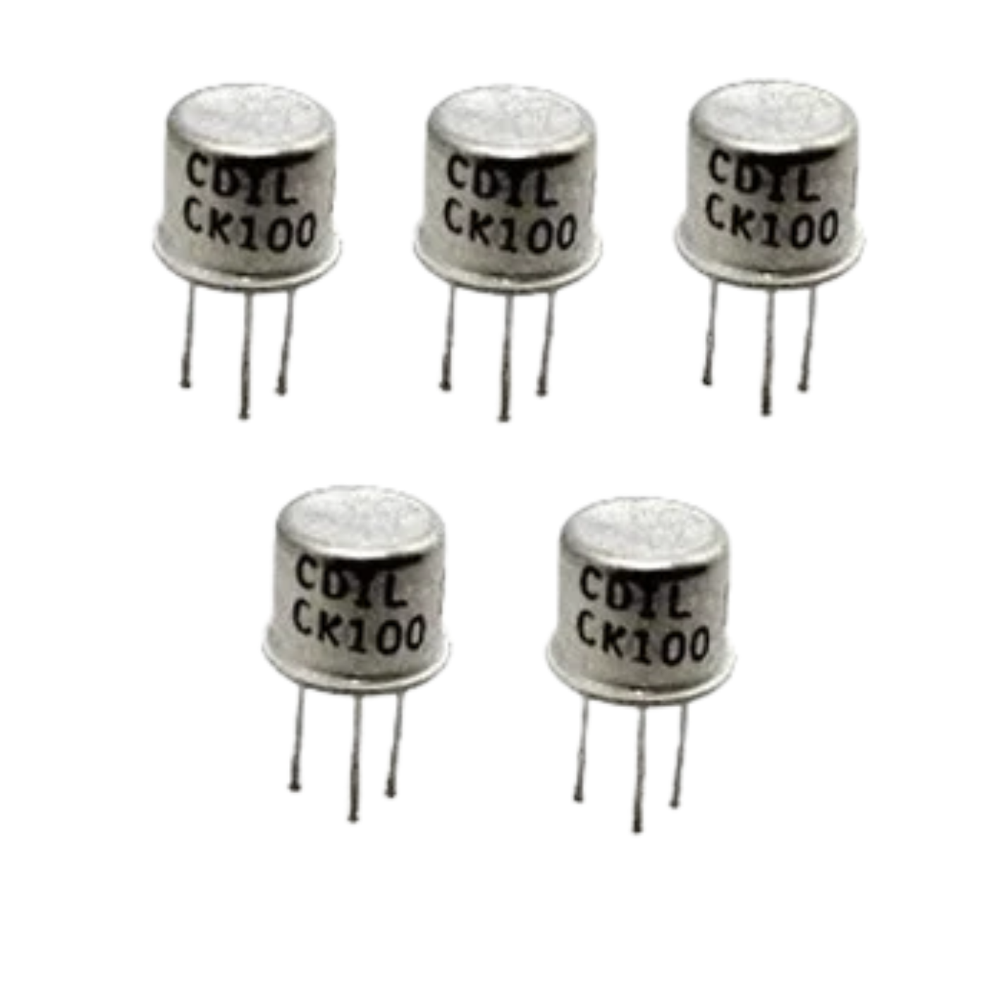
CDIL CK100 PNP Silicon Planar…
CDIL CK100 PNP Silicon Planar Power Transistor
The CK100 Transistor by CDIL is a versatile, general-purpose medium power PNP silicon planar transistor designed for both switching and amplifier applications.
Built with a robust three-layer construction, it operates efficiently within its working range, where the collector current (IC) is directly influenced by changes in the base current (IB) for a given collector-emitter voltage (VCE).
This allows for consistent and reliable amplification in a wide variety of electronic circuits. Known for its dependable performance, the CK100 is widely used in hobby electronics, educational projects, and industrial applications requiring a medium power transistor solution.
Features:
High Ruggedness.
Simple driving requirements.
The highly secure operating location
For minimal distortion complementary designs.
Easy to transport and handle.
Applications:
General-purpose switching and amplification.
General Purpose Medium Power Transistor
₹20.32
MRP. ₹47.60
Incl. GST (No Hidden Charges)
Incl. GST (No Hidden Charges)
CDIL CK100 PNP Silicon Planar Power Transistor
CDIL CK100 PNP Silicon Planar Power Transistor The CK100 Transistor by CDIL is a versatile, general-purpose medium power PNP silicon planar transistor designed for both switching and amplifier applications. Built …
As low as
₹20.32
₹20.32
MRP. ₹47.60
Incl. GST (No Hidden Charges)
