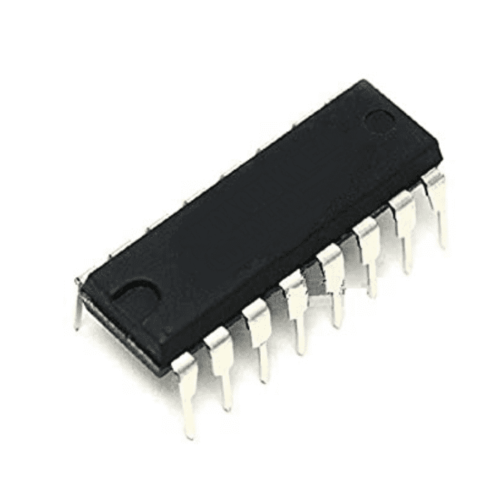
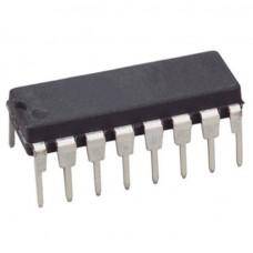
My Menu
DS1307 Real Time Clock Module
(0)
DS1307 Real Time Clock Module The DS1307 is a low-power clock/calendar with 56 bytes of battery backup SRAM. The clock/calendar provides seconds, minutes, hours, day, date, month and year-qualified data. The end date of each month is automatically adjusted, especially for months with less than 31 days. This is Tiny RTC Real Time Clock DS1307 I2C IIC Module for Arduino . It contains a DS1307 real-time clock IC . It’s one of the easiest to use RTCs out there, with Arduino and other libraries or simply use I2C commands to set and retrieve the time and date. Along with the …
Condition: NEW
As low as ₹42,67   MRP. ₹96,60 Incl. GST (No Hidden Charges)
IN STOCK
For bulk orders or wholesale inquiries, please contact us at Email or call/message us at Phone.

DS1307 Real Time Clock Module The DS1307 is a low-power clock/calendar with 56 bytes of battery backup SRAM. The clock/calendar provides seconds, minutes, hours, day, date, month and year-qualified data. The end date of each month is automatically adjusted, especially for months with less than 31 days. This is Tiny RTC Real Time Clock DS1307 I2C IIC Module for Arduino . It contains a DS1307 real-time clock IC . It’s one of the easiest to use RTCs out there, with Arduino and other libraries or simply use I2C commands to set and retrieve the time and date. Along with the DS1307 real-time clock, the module also has an Atmel 24C32 EEPROM chip which is handy for storing data without worrying about power loss. There is also space on the board to solder your own DS18B20 temperature sensor. DS1307 Real Time Clock module is used to track the current time and date. It is generally used in computers, laptops, mobiles, embedded system applications devices, etc. In many embedded systems, we need to put timestamps while logging data i.e. sensor values, GPS coordinates, etc. For getting timestamps, we need to use RTC (Real Time Clock). This module is based on the DS1307 IC from Dallas. It uses a 32.768 kHz clock. And supports I2C Interface. Pinout of DS1307: Pinout of DS1307 Real Time Clock Module Pin 1, 2: Connections for standard 32.768 kHz quartz crystal. The internal oscillator circuitry is intended for operation with a crystal having a specified load capacitance of 12.5pF. X1 is the input to the oscillator and can alternatively be connected to an external 32.768 kHz oscillator. The output of the internal oscillator, X2 is drifted if an external oscillator is connected to X1. Pin 3 : Battery input for any standard 3V lithium cell or another energy source. Battery voltage should be between 2V and 3.5V for suitable operation. The nominal write-protect trip point voltage at which access to the RTC and user RAM is denied is set by the internal circuitry as 1.25 x VBAT nominal. A lithium battery with 48mAhr or greater will back up the DS1307 for more than 10 years in the absence of power at 25ºC. UL is recognized to ensure against reverse charging current when utilized as part of conjunction with a lithium battery. Pin 4: Ground. Pin 5: Serial data input/output. The input/output for the I2C serial interface is the SDA, which is the open drain and requires a pull-up resistor, allowing a pull-up voltage of 5.5V. Regardless of the voltage on VCC. Pin 6: Serial clock input. It is the I2C interface clock input and is used in data synchronization. Pin 7: Square wave/output driver. When enabled, the SQWE bit set to 1, the SQW/OUT pin outputs one of four square-wave frequencies (1Hz, 4 kHz, 8 kHz, and 32 kHz). This is also an open drain and requires an external pull-up resistor. It requires the application of either Vcc or Vb at to operate SQW/OUT, with an allowable pull-up voltage of 5.5V and can be left floating, if not used. Pin 8: Primary power supply. When the voltage is applied within normal limits, the device is fully accessible and data can be written and read. When a backup supply is connected to the device and VCC is below VTP, read and write are inhibited. However, at low voltages, the timekeeping function still functions.

  • Two-wire I2C interface
  • Hour: Minutes: Seconds AM/PM
  • Leap year compensation
  • Accurate calendar up to the year 2100
  • Consumes Less than 500nA in Battery-Backup
  • 56 Bytes of Non-volatile memory available to the user
  • 4KB of serial electrically erasable and programmable read-only memory (EEPROM)
  • Embed DS18B20 temperature sensor interface with the pull-up resistor.
  • Operating Voltage 5V
  • Battery IR2032
  • Dimensions 2.7 x 2.8cms
  • Weight 5 grams
To rate this product please login!

Related products

Related products

CMOS Hex Buffers/Converter IC…
(0)
CMOS Hex Buffers/Converter IC - CD4009 CD4009 Hex Buffer/Converters may be used as CMOS to TTL or DTL logic-level converters or CMOS high-sink-current drivers. The CD4009 types are supplied in 16-lead hermetic dual-in-line ceramic packages (F3A suffix), 16-lead dual-in-line plastic packages (E suffix). check out : CMOS 8-Input NAND/AND Gate IC - CD4068 Applications: CMOS to DTL/TTL hex converter CMOS current "sink" or "source" driver CMOS high-to-low logic-level converter Multiplexer — 1 to 6 or 6 to 1 check out : Hex Buffer/Converter IC - CD4010
₹27,43   MRP. ₹47,60
Incl. GST (No Hidden Charges)
CMOS 8-Input NAND/AND Gate IC…
(0)
CMOS 8-Input NAND/AND Gate IC - CD4068 The CD4068 CMOS 8-Input NAND/AND gate IC (Integrated Circuits) provides the system designer with direct implementation of the positive logic 8-Input NAND and AND functions and supplements the existing family of CMOS gates. The CD4x Series CD4068 is an 8-Input NAND/AND Gate CMOS logic-based IC belonging to a CD4000 series of integrated circuits. Firstly, Two output options are available such as AND and NAND gate. Secondly, the same input pins deliver both logical functions. It is available in a variety of packages which includes 14-pin PDIP, GDIP, PDSO. The typical operating voltage of the IC is +5V, but it can also be operated +10V and +15V. It has a standard symmetric output. This IC is useful for applications requiring low power. Furthermore, it offers a wide voltage operating range. check out : CMOS Hex Buffers/Converter IC - CD4009 Pinout: Pinout of CD4068
₹25,39   MRP. ₹54,60
Incl. GST (No Hidden Charges)
CD4029 - Binary Decade Up-Dow…
(0)
CD4029 - Binary Decade Up-Down Counter IC The CD4029 IC consists of a four-stage binary or BCD-decade up/ down counter with provisions for look-ahead carry in both counting modes. The inputs consist of a single CLOCK, CARRY-IN (CLOCK ENABLE), BINARY/DECADE, UP/DOWN, PRESET ENABLE, and four individual JAM signals. Q1, Q2, Q3, Q4, and a CARRY OUT signal are provided as outputs. A high PRESET ENABLE signal allows information on the JAM INPUTS to preset the counter to any state asynchronously with the clock. A low on each JAM line, when the PRESET-ENABLE signal is high, resets the counter to its zero counts. The counter is advanced one count at the positive transition of the clock when the CARRY-IN and PRE-SET ENABLE signals are low. Advancement is inhibited when the CARRY-IN or PRESET ENABLE signals are high. The CARRY-OUT signal is normally high and goes low when the counter reaches its maximum count in the UP mode or the minimum count in the DOWN mode provided the CARRY-IN signal is low. The CARRY-IN signal in the low state can thus be considered a CLOCK ENABLE. The CARRY-IN terminal must be connected to VSS when not in use. Binary counting is accomplished when the BINARY/DECADE input is high; the counter counts in the decade mode when the BINARY/DECADE input is low. The counter counts up when the UP/DOWN input is high, and down when the UP/DOWN input is low. Multiple packages can be connected in either a parallel clocking or a ripple-clocking arrangement as shown in Figure 17. Parallel clocking provides synchronous control and hence faster response from all counting outputs. Ripple-clocking allows for longer clock input rise and fall times. The CD4x Series CD4029 is supplied in these 16-lead outline packages: Braze Seal DIP H4X Frit Seal DIP H1F Ceramic Flatpack H6W. Pinout: Pinout of CD4029 IC
₹38,61   MRP. ₹61,60
Incl. GST (No Hidden Charges)
555 Timer IC
(0)
555 Timer IC The 555 timer IC is an integrated circuit (chip) used in a variety of timer, pulse generation, and oscillator applications. The ic 555 can be used to provide time delays, as an oscillator, and as a flip-flop element. Derivatives provide up to four timing circuits in one package. These 555 timer ICs are precision timing circuits capable of producing accurate time delays or oscillations. 
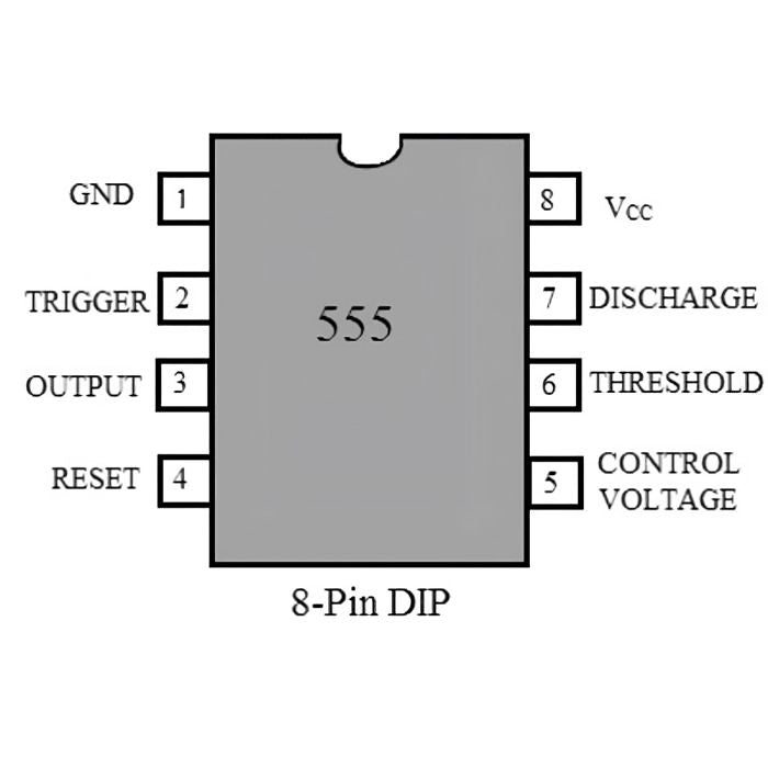
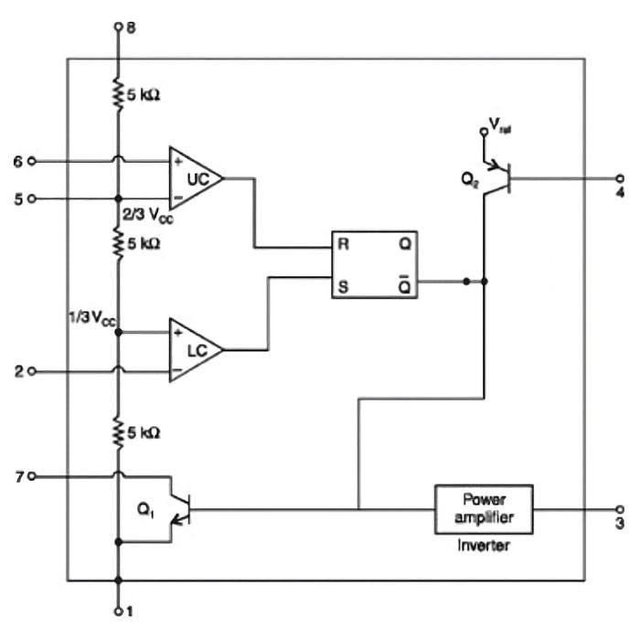
In the time-delay or monostable mode of operation, the timed interval is controlled by a single external resistor and capacitor network. In the astable mode of operation, the frequency and duty cycle can be controlled independently with two external resistors and a single external capacitor. The threshold and trigger levels normally are two-thirds and one-third, respectively, of VCC. These levels can be altered by the use of the control voltage terminal. When the trigger input falls below the trigger level, the flip-flop is set and the output goes high. If the trigger input is above the trigger level and the threshold input is above the threshold level, the flip-flop is reset and the output is low. The reset (RESET) input can override all other inputs and can be used to initiate a new timing cycle. When RESET goes low, the flip-flop is reset and the output goes low. When the output is low, a low-impedance path is provided between discharge (DISCH) and ground. The output circuit is capable of sinking or sourcing current up to 200 mA. The operation is specified for supplies of 5 V to 15 V. With a 5-V supply, output levels are compatible with TTL inputs. The NE555 is characterized for operation from 0°C to 70°C. This is characterized for operation from –40°C to 85°C. The NE555 is characterized for operation over the full military range of –55°C to 125°C. Features of the 555 timers are: Supply voltage between 4.5 and 18 volts. supply current 3 to 6 mA, and a Rise/Fall time of 100 nSec.
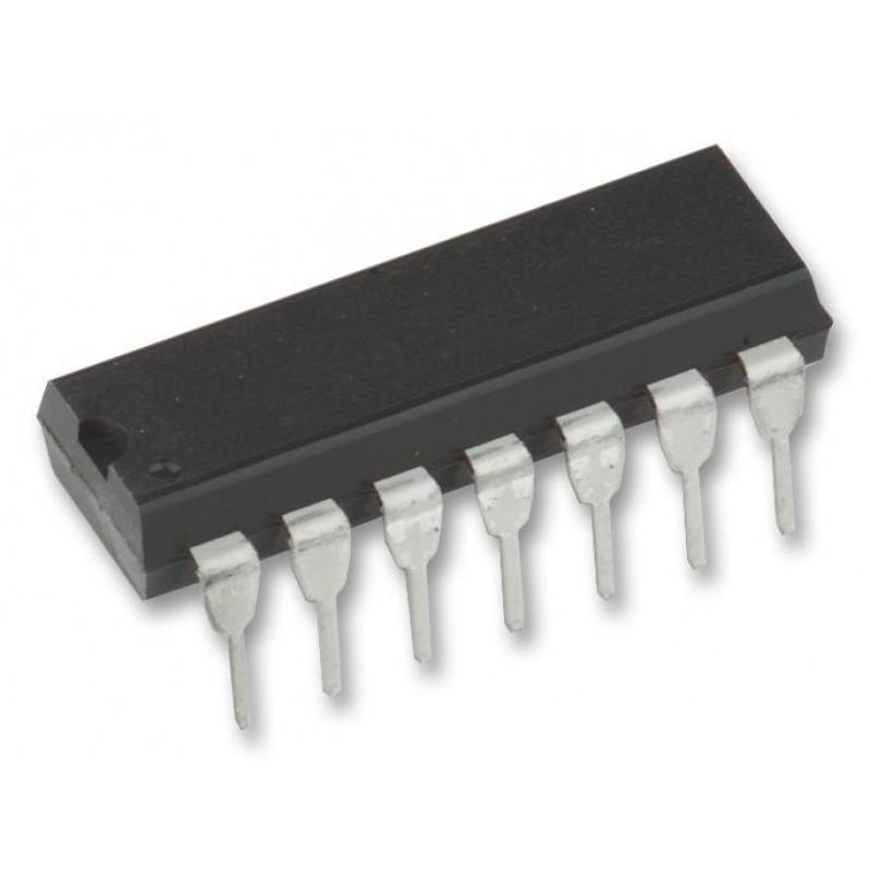
 IC 555 pin diagram The IC 555 is used in many circuits, for example, a One-shot pulse generator in Monostable mode as an Oscillator in Astable Mode or in Bistable mode to produce a flip/flop type action. It is also used in many types of other circuits for the achievement of various purposes for instance Pulse Amplitude Modulation (PAM), Pulse Width Modulation (PWM), etc. This IC 555 can be configured to use as a monostable multivibrator, an astable multivibrator. If you want to use this 555 timer ic in your projects, there are a few essential components that are helpful are breadboard or vero board , switch , jumper wires , resistors , capacitors and batteries . Features: Adjustable Duty Cycle. Precision timing circuits capable of producing accurate time delays or oscillations. Can be configured as a monostable multivibrator, astable multivibrator, or in bistable mode. Features a control voltage terminal to alter threshold and trigger levels. RESET input for initiating a new timing cycle. Rise/Fall time of 100 nSec. Applications: The IC 555 is used for Tone generation. It is used to make an alarm circuit. They are also used for frequency division applications. The IC 555 is used as a relaxation oscillator. They are also used in digital counter circuits. IC 555 is widely used for electronics projects. Also check 8 Pin DIP IC Socket Base Adaptor available on the Iotcart website. it is designed for 8-pin integrated circuits (ICs) commonly used in electronic devices like timers, oscillators, and digital logic circuits. The socket has a molded notch for proper orientation, making it easy to insert and remove ICs
₹8,13   MRP. ₹16,80
Incl. GST (No Hidden Charges)
CD4099 - 8 bit Addressable La…
(0)
CD4099 - 8 bit Addressable Latch IC The CD4099 8-bit addressable latch IC is a serial-input, parallel-output storage register that can perform a variety of functions. Data are inputted to a particular bit in the latch when that bit is addressed (by means of input A0, A1, A2) and when WRITE DISABLE is at a low level. When WRITE DISABLE is high, data entry is inhibited; however, all 8 outputs can be continuously read independently of WRITE DISABLE and address inputs. A master RESET input is available, which resets all bits to a logic "0" level when RESET and WRITE DISABLE is at a high level. When RESET is at a high level, and WRITE RESET is at a low level, the latch acts as a 1-of-8 demultiplexer; the bit that is addressed has an active output that follows the data input, while all unaddressed bits are held to a logic "0" level. The CD4099 types are supplied in 16-lead hermetic dual-in-line ceramic packages (F3A suffix), 16-lead dual-in-line plastic packages (E suffix), 16-lead small-outline packages (M, M96, MT, and NSR suffixes), and 16-lead thin shrink small-outline packages (PW and PWR suffixes). check out : Quad NOR R-S Latch Tri-state IC - CD4043 Pinout: Pin No Pin Name Description 1 Q7 Output Pin 7 of Latch 2 CL Clear Output Pin 3 D Data Input 4 E’ Enable Pin 5 A0 Input Pin 0 of Latch 6 A1 Input Pin 1 of Latch 7 A2 Input Pin 2 of Latch 8 VSS Source Supply 9 Q0 Output Pin 0 of Latch 10 Q1 Output Pin 1 of Latch 11 Q2 Output Pin 2 of Latch 12 Q3 Output Pin 3 of Latch 13 Q4 Output Pin 4 of Latch 14 Q5 Output Pin 5 of Latch 15 Q6 Output Pin 6 of Latch 16 VDD Drain Supply Applications: Multi-line decoders A/D converters
₹26,42   MRP. ₹49,00
Incl. GST (No Hidden Charges)
CD4514 - 4 Bit Latch/4-16 Lin…
(0)
CD4514 - 4 Bit Latch/4-16 Line Decoder IC The CD4x Series CD4514 IC is a 4-to-16-line decoder with latched inputs implemented with complementary MOS (CMOS) circuits constructed with N- and P-channel enhancement mode transistors. These circuits are primarily used in decoding applications where low power dissipation and/or high noise immunity are required. The CD4514 (output active high option) presents a logical “1” at the selected output. The input latches are R–S type flip-flops, which hold the last input data presented prior to the strobe transition from “1” to “0”. This input data is decoded and the corresponding output is activated. An output inhibits line is also available. Pinout: Pinout Of CD4514 IC
₹166,62   MRP. ₹278,60
Incl. GST (No Hidden Charges)
CD4040 - 12-Stage Ripple Carr…
(0)
CD4040 - 12-Stage Ripple Carry Binary Counter IC The CD4x Series CD4040 is a ripple-carry binary counter that features 12 stages, push-pull type, and balanced outputs, with standard speed (TPD > 50ns). All counter stages are master-slave flip-flops. Supports wide input voltage ranges from 3V to 18V. The maximum input current at 18V is 1 uA whereas 100 nA at 18V and 25°C. All counter stages are master-slave flip-flops. The state of a counter advances one count on the negative transition of each input pulse; a high level on the RESET line resets the counter to its all-zeros state. Schmitt's trigger action on the input-pulse line permits unlimited rise and fall times. All inputs and outputs are buffered. 16 Pin DIP is available in a hermetic dual-in-line ceramic package. We also have a CD4020 with similar features. The differences are CD4020 is a 14 Stage binary counter whereas CD4040 is a 12 Stage binary counter and there is a difference between the pin layout. check out : CD4518 - Dual BCD Up Counter IC (Original) Pinout: Pinout of CD4040 IC Applications: Control Counters Timers Frequency Dividers Time-Delay Circuits
₹28,45   MRP. ₹47,60
Incl. GST (No Hidden Charges)
16-Channel Analog Multiplexer…
(0)
16-Channel Analog Multiplexer/Demultiplexer IC - CD4067 CD4067 CMOS analog multiplexers/demultiplexers are digitally controlled analog switches having low ON impedance, low OFF leakage current, and internal address decoding. In addition, the ON resistance is relatively constant over the full input-signal range. The CD4067 is a 16-channel multiplexer with four binary control inputs, A, B, C, D, and an inhibit input, arranged so that any combination of the inputs selects one switch. A logic “1” present at the inhibit input turns all channels off. The CD4067 type are supplied in 24-lead hermetic dual-in-line ceramic packages (F3A suffix), 24-lead dual-in-line plastic packages (E suffix), 24-lead small-outline packages (M, M96, and NSR suffixes), and 24-lead thin shrink small-outline packages (P and PWR suffixes). check out : CD4066 - Quad Bilateral Switch IC Applications: Analog and digital multiplexing and demultiplexing A/D and D/A conversion Signal gating
₹166,62   MRP. ₹278,60
Incl. GST (No Hidden Charges)
CD4081 - Quad 2 Input AND Gat…
(0)
CD4081 - Quad 2 Input AND Gate IC CD4081 Quad 2 Input AND gates IC provides the system designer with direct implementation of the AND function and supplements the existing family of CMOS gates. The CD4081 types are supplied in 14-lead hermetic dual-in-line ceramic packages (F3A suffix), 14-lead dual-in-line plastic packages (E suffix), 14-lead small-outline packages (M, MT, M96, and NSR suffixes), and 14-lead thin shrink small-outline packages (PW and PWR suffixes). check out : CD4532 - 8 Bit Priority Encoder IC (Original) Pinout: Pinout Of CD4081 IC check out : CD4030 - Quad 2-Input Exclusive OR (EXOR) Gate IC
₹17,28   MRP. ₹42,00
Incl. GST (No Hidden Charges)
Mastech MS2001C AC Digital Cl…
(0)
Mastech MS2001C AC Digital Clamp Meter Mastech MS2001 Digital AC/DC Clamp Meter is a handheld 3 1/2 digital clamp meter for measuring DC and AC voltage, AC current, Resistance, Diode and Continuity Test with battery operated.  Mastech Clamp meters are used by electricians, sometimes with the clamp incorporated into a general purpose multimeter. It is simple to measure very high currents (hundreds of amperes) with the appropriate current transformer. Check replaceable fuses ; Please make sure to connect the testing wires to right terminals ; Select the appropriate range of measurement (that is selecting the measurement range from highest to smallest if the range is unknown). check out : MECO-603 Digital Multimeter
₹2731,97   MRP. ₹5878,60
Incl. GST (No Hidden Charges)
14 Stage Ripple Carry Binary …
(0)
14 Stage Ripple Carry Binary Counter IC - CD4020 The CD4020 IC is a ripple-carry binary counter. All counter stages are master-slave flip-flops. The state of a counter advances one count on the negative transition of each input pulse; a high level on the RESET line resets the counter to its all-zeros state. Schmitt's trigger action on the input-pulse line permits unlimited rise and fall times. All inputs and outputs are buffered. The CD4x Series CD4020 type is supplied in 16-lead hermetic dual-in-line ceramic packages (F3A suffix), 16-lead dual-in-line plastic packages (E suffix), 16-lead small-outline packages (NSR suffix), and 16-lead thin shrink small-outline packages (PW and PWR suffixes). check out : CD4040 - 12-Stage Ripple Carry Binary Counter IC Pinout: Pinout of CD4020 IC Applications: Control counters Timers Frequency dividers Time-delay circuits
₹19,30   MRP. ₹44,80
Incl. GST (No Hidden Charges)
Triple 3-Input AND Gate IC - …
(0)
Triple 3-Input AND Gate IC - CD4073 The CD4073 IC is a Triple 3-input AND Gate made by using the complimentary MOS (CMOS) technology integrated with P and N-type MOSFETS. This IC allows system designers to utilize the AND gate function and supplement the existing family of CMOS gates. The IC offers a wide array of workable voltages and conditions making it easy to use with different DLD configurations. The output of the IC is always available in TTL, allowing it to be easily interfaceable with CMOS, NMOS, and other TTL devices. CD4073 AND gates, provide the system designer with direct implementation of the AND function and supplement the existing family of CMOS gates. The CD4x Series CD4073 types are supplied in 14-lead hermetic dual-in-line ceramic packages (F3A suffix), 14-lead dual-in-line plastic packages (E suffix), 14-lead small-outline packages (M, MT, M96, and NSR suffixes), and 14-lead thin shrink small-outline packages (PW and PWR suffixes). check out : Triple 3-Input NAND Gate IC - CD4023 Pinout: Pinout of CD4073 IC Pin Name Pin # Type Description VDD 14 Power Supply Voltage (+3 to +15V) GND 7 Power Ground (0V) A1 to A3 1, 3, 13 Input Inputs A of the three AND gates B1 to B3 2, 4, 12 Input Inputs B of the three AND gates C1 to C3 5, 8, 11 Input Inputs C of the three AND gates Q1 to Q3 6, 9, 10 Output Outputs from the three AND gates
₹28,45   MRP. ₹47,60
Incl. GST (No Hidden Charges)
CD4066 - Quad Bilateral Switc…
(0)
CD4066 - Quad Bilateral Switch IC The CD4066 device is a quad bilateral switch intended for the transmission or multiplexing of analog or digital signals. It is pin-for-pin compatible with the CD4016 device but exhibits a much lower on-state resistance. In addition, the on-state resistance is relatively constant over the full signal-input range. The CD4x Series CD4066 device consists of four bilateral switches, each with independent controls. Both the p and the n devices in a given switch are biased on or off simultaneously by the control signal. The well of the n-channel device on each switch is tied to either the input (when the switch is on) or to V SS (when the switch is off). This configuration eliminates the variation of the switch-transistor threshold voltage with the input signal and, thus, keeps the on-state resistance low over the full operating-signal range. The advantages over single-channel switches include peak input-signal voltage swings equal to the full supply voltage and more constant on-state impedance over the input-signal range. However, for sample-and-hold applications, the CD4016 device is recommended. check out : CD4016 - Quad Bilateral Switch IC Pinout: Pinout of CD4066 IC
₹16,26   MRP. ₹40,60
Incl. GST (No Hidden Charges)
CD4504 - Hex Voltage Level Sh…
(0)
CD4504 - Hex Voltage-Level Shifter IC The CD4504 hex voltage level shifter IC consists of six circuits that shift input signals from the V CC logic level to the V DD logic level. To shift TTL signals to CMOS logic levels, the SELECT input is at the V CC HIGH logic state. When the SELECT input is in a LOW logic state, each circuit translates signals from one CMOS level to another. The CD4504 types are supplied in 16-lead hermetic dual-in-line ceramic packages (F3A suffix), 16-lead dual-in-line plastic packages (E suffix), 16-lead small-outline packages (M, M96, and MT suffixes), and 16-lead thin shrink small-outline packages (PW and PWR suffixes). Pinout: Pin No Pin Name Description 1 VCC Collector supply voltage 2 AOUT output of level shifter A 3 AIN input of level shifter A 4 BOUT output of level shifter B 5 BIN input of level shifter B 6 COUT output of level shifter C 7 CIN input of level shifter C 8 VSS source supply 9 DIN input of level shifter D 10 DOUT output of level shifter D 11 EIN input of level shifter E 12 EOUT output of level shifter E 13 SELECT select pin 14 FIN input of level shifter F 15 FOUT output of level shifter F 16 VDD Drain supply
₹28,45   MRP. ₹49,00
Incl. GST (No Hidden Charges)
Divide by 8 Counter/Divider I…
(0)
Divide by 8 Counter/Divider IC - CD4022 The CD4022 IC is a 4-stage divide-by-8 Johnson counter with 8 decoded outputs and a carry-out bit. These counters are cleared to their zero counts by a logical ‘‘1’’ on their reset line. These counters are advanced on the positive edge of the clock signal when the clock enable signal is in the logical ‘‘0’’ state. The configuration of the CD4x Series CD4022 permits medium-speed operation and assures a hazard-free counting sequence. The 10/8 decoded outputs are normally in the logical ‘‘0’’ state and go to the logical ‘‘1’’ state only at their respective time slot. Each decoded output remains high for 1 full clock cycle. The carry-out signal completes a full cycle for every 10/8 clock input cycle and is used as a ripple to carry the signal to any succeeding stages. check out : 8-bit Up/Down Binary Counter IC - CD40193 Pinout: Pinout of CD4022 IC
₹20,32   MRP. ₹47,60
Incl. GST (No Hidden Charges)

Features

icon

Full Screen mode

Mode
On
Off

Dark mode

Mode
On
Off

Clear local storage

Clear Cache & Default
0