

Sort by
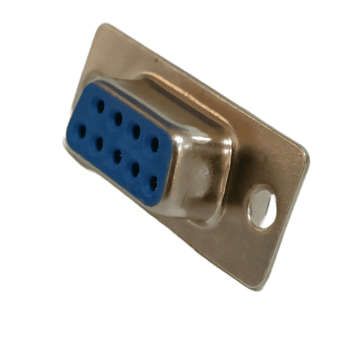
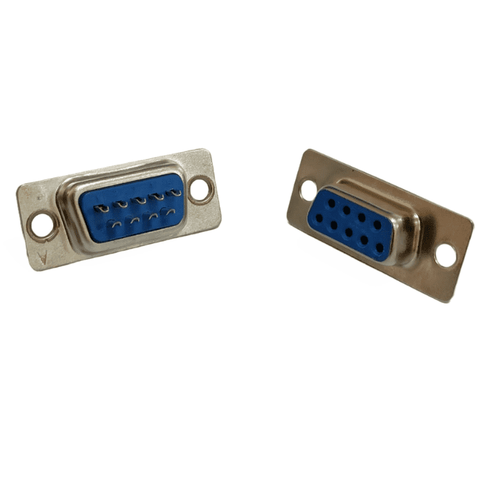
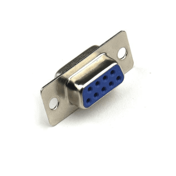
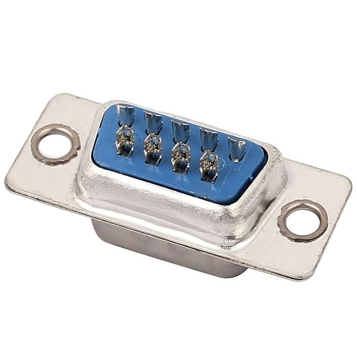
DB9 Female Straight Connector
DB9 Female Straight Connector
The most popular kind of electrical connector is DB9 Female straight Connector. The D-sub minuscule (D-sub) connector plug and socket family includes the DB 9 connector, which is used with computers and other communication equipment. A five-pin row sits above a four-pin row in the arrangement of DB-9 pins, which are organized in rows of two.
The EIA/TIA 232 serial interface standard established the purpose of each of the nine pins as a standard so that different manufacturers may incorporate them into their products. DB9 connections are made to work with this standard. Keyboards, mouse, joysticks, and other serial peripheral devices were frequently connected using these
connectors
. For data communication, they are also utilized in DB9 cable assemblies.
Today, more advanced interfaces like USB, PS/2, Firewire, and others have mostly taken the place of the DB9. However, the DB9 interface is still widely used by many vintage devices for serial communication.
Applications:
Network ports.
Computer video output.
Game controller ports.
Linear and rotary encoders in industries.
₹11,13
MRP. ₹32,20
Incl. GST (No Hidden Charges)
Incl. GST (No Hidden Charges)
DB9 Female Straight Connector
DB9 Female Straight Connector The most popular kind of electrical connector is DB9 Female straight Connector. The D-sub minuscule (D-sub) connector plug and socket family includes the DB 9 connector, …
As low as
₹11,13
₹11,13
MRP. ₹32,20
Incl. GST (No Hidden Charges)
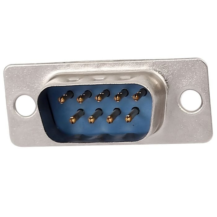
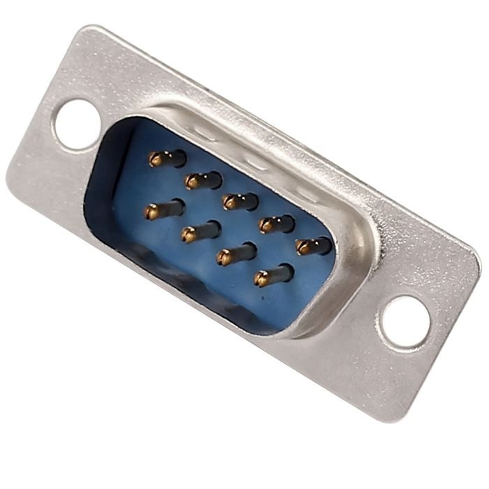
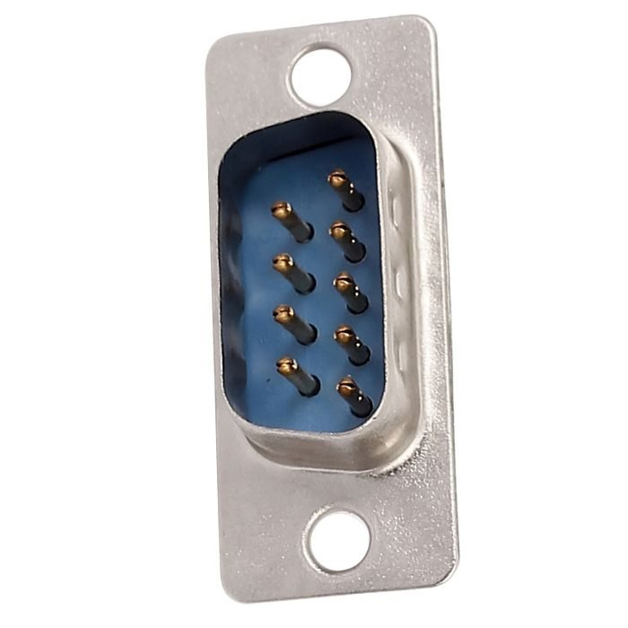
DB9 Male Straight Connector
DB9 Male Straight Connector
The most common type of electrical connector is the DB9 male Welded Connector. The D-sub miniature (D-sub) connector plug and socket family for computer and communication devices includes the DB 9 connector. DB-9 pins are organized in two-row rows, with one five-pin row above a four-pin row.
The EIA/TIA 232 serial interface standard determined the function of all nine pins as a standard so that multiple companies could design them into their products, and DB9 connectors are designed to work with it. DB9 connectors were widely used for serial peripheral devices such as keyboards, mice, joysticks, and so on. They are also used for data connectivity in DB9 cable assemblies.
check out :
Male to Male DB-9 Cable
Features:
Solder cup configuration for longevity.
Nickel-plated terminals.
Gold plated pins and Good quality.
₹23,36
MRP. ₹44,80
Incl. GST (No Hidden Charges)
Incl. GST (No Hidden Charges)
DB9 Male Straight Connector
DB9 Male Straight Connector The most common type of electrical connector is the DB9 male Welded Connector. The D-sub miniature (D-sub) connector plug and socket family for computer and communication …
As low as
₹23,36
₹23,36
MRP. ₹44,80
Incl. GST (No Hidden Charges)
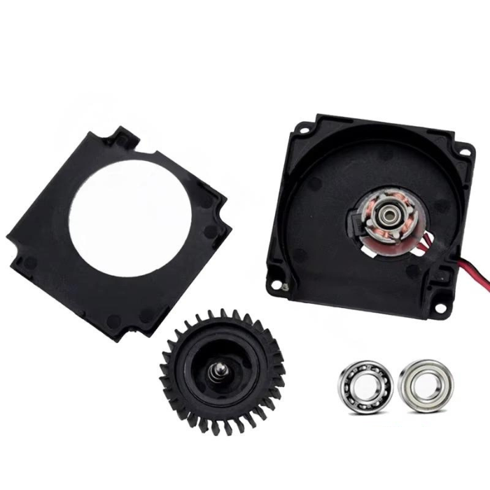
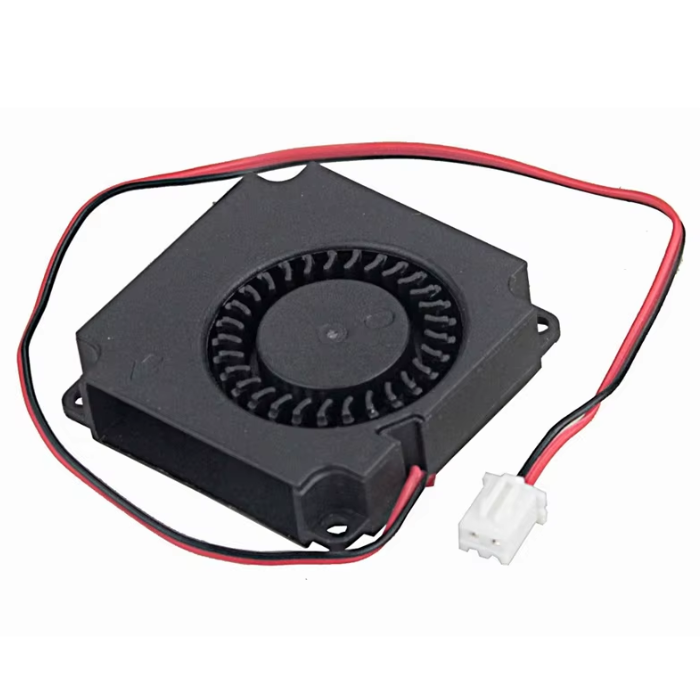
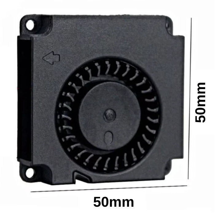
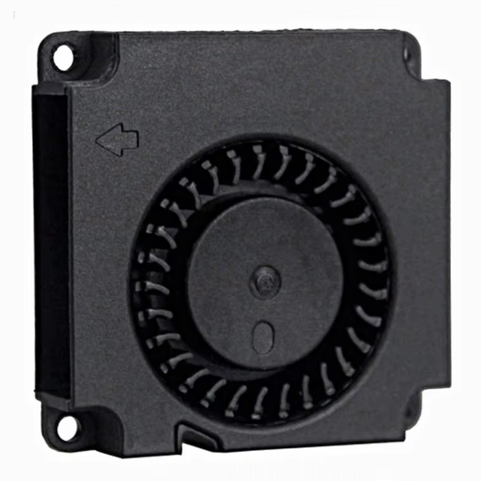
DC 12V 4CM 5010 Double Ball C…
DC 12V 4CM 5010 Double Ball Cooling Fan Durable Turbo Blower for 3D Printer
The Original DC 12V 4CM 5010 Double Ball Cooling Fan is a great choice for a strong and easy-to-use fan for your 3D printer. It runs at 5000 to 6000 RPM to keep things cool and has five durable blades. The 2-pin connection makes it simple to plug in, and it works well for 3D printer cases or other electronics that need reliable cooling.
₹110,16
MRP. ₹208,60
Incl. GST (No Hidden Charges)
Incl. GST (No Hidden Charges)


DC 12V 4CM 5010 Double Ball Cooling Fan Durable Turbo Blower for 3D Printer
DC 12V 4CM 5010 Double Ball Cooling Fan Durable Turbo Blower for 3D Printer The Original DC 12V 4CM 5010 Double Ball Cooling Fan is a great choice for a …
As low as
₹110,16
₹110,16
MRP. ₹208,60
Incl. GST (No Hidden Charges)
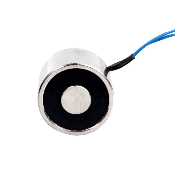
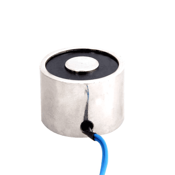
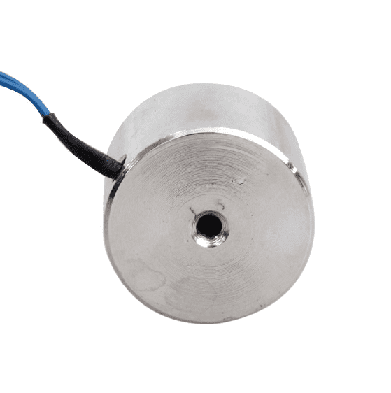
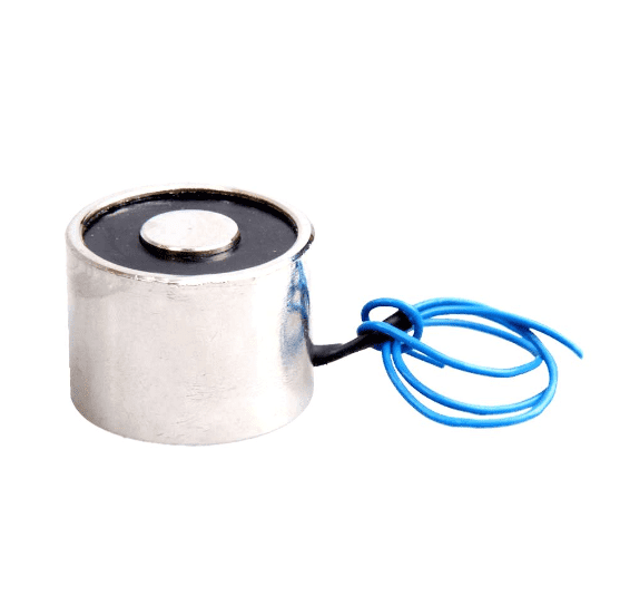
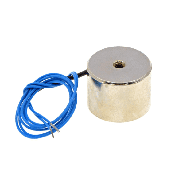
DC 12V KK-P25/20 8KG Lifting …
DC 12V KK-P25/20 8KG Lifting Solenoid Electromagnet
This DC 12V KK-P25/20 8KG Lifting Solenoid Electromagnet consists of an iron core and a coil to attract magnetic substances, using the magnetic action induced by electric current, only while the current is applied. This compact functional device offers high power with high reliability. The structure and design to release the residual magnetism left after de-energization is also one of its unique features.
Working Principle:
An electromagnet is simply a coil of wire. It is usually wound around an iron core. However, it could be wound around an air core, in which case it is called a solenoid. When connected to a DC voltage or current source, the electromagnet becomes energized, creating a magnetic field just like a permanent magnet. The magnetic flux density is proportional to the magnitude of the current flowing in the wire of the electromagnet.
The polarity of the electromagnet is determined by the direction of the current. The north pole of the electromagnet is determined by using your right hand. Wrap your fingers around the coil in the same direction as the current is flowing (conventional current flows from + to -). The direction your thumb is pointing in the direction of the magnetic field so north would come out of the electromagnet in the direction of your thumb. DC electromagnets are principally used to pick up or hold objects.
Precaution:
Electromagnets must meet the following conditions to achieve maximum suction:
The object to be sucked must have good magnetic permeability.
Proper use of power supply, rated voltage.
The object to be sucked must be flat and clean.
The object to be sucked must be greater than or equal to the surface of the magnet( For example the magnet is 20 x 15 mm, so the surface area is S=r²?=10²? mm² so the object to be sucked must be greater than or equal to 10²? mm² )
The object to be sucked must be greater than 5mm. (If the thickness decreases, the suction decreases)
The object to be sucked must be close, the middle can’t be interspersed with objects or gaps
Suction means more than 5cm in thickness, and surface roughness, the surface is greater than the cross-sectional area of the electromagnet and maximum suction completely fits together on an iron-based material.
Electromagnet in working conditions electromagnetic conversion would produce a certain amount of heat, electricity more frequently the higher temperature, which is a normal phenomenon.
₹262,61
Incl. GST (No Hidden Charges)
Out of Stock
MRP. ₹558,60
Incl. GST (No Hidden Charges)
DC 12V KK-P25/20 8KG Lifting Solenoid Electromagnet
DC 12V KK-P25/20 8KG Lifting Solenoid Electromagnet This DC 12V KK-P25/20 8KG Lifting Solenoid Electromagnet consists of an iron core and a coil to attract magnetic substances, using the magnetic …
As low as
₹262,61
₹262,61
MRP. ₹558,60
Incl. GST (No Hidden Charges)
Out of Stock
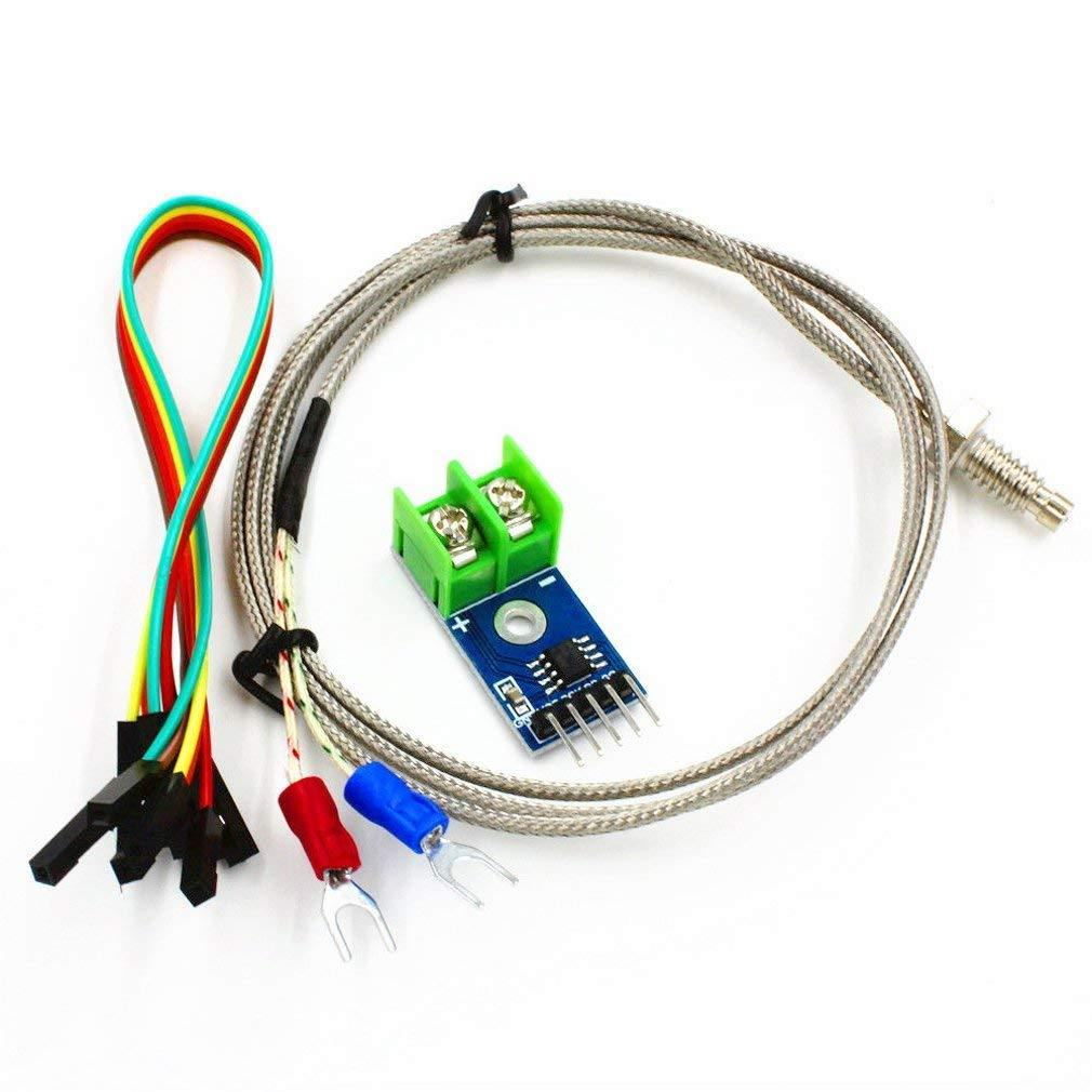
DC 3-5V MAX6675 Module + K Ty…
DC 3-5V MAX6675 Module + K Type Thermocouple Temperature Sensor Thermocouple Sensor Set M6 Screw and Jumper Wire F to F
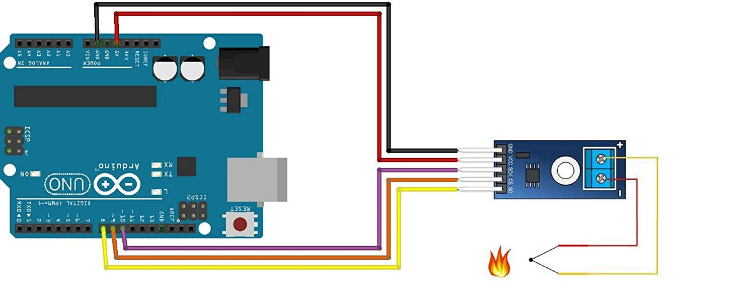
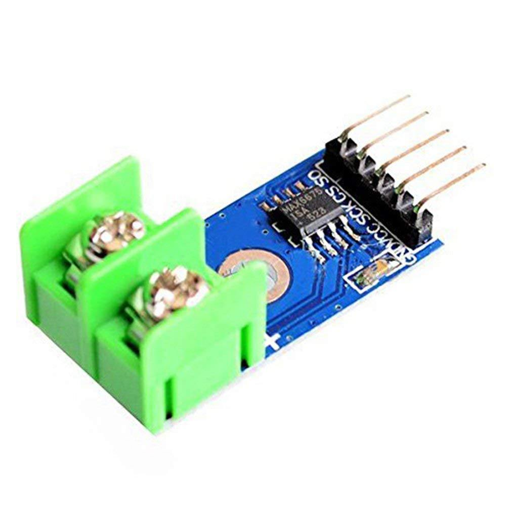
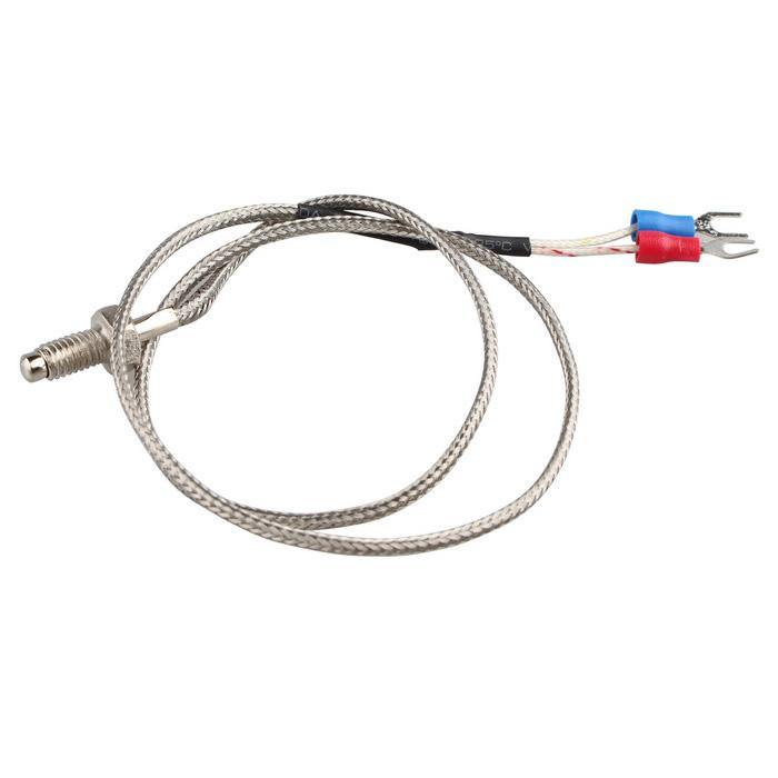
This MAX6675 Module + K Type Thermocouple Sensor Measure 1024°C Temperature sensor makes use of the Maxim MAX6675 K-Thermocouple to digital converter IC to provide a microcontroller compatible digital serial interface (SPI compatible) for giving an accurate temperature compensated measurement of the supplied K-Type thermocouple sensor.
It has a 12-bit resolution providing temperature readings from 0°C to 1024°C (max temperature of the supplied
sensor
is 450°C) with a resolution of 0.25°C.
Screw terminals allow for connection to the thermocouples spade connectors and a 5 pin standard 0.1? header provides an interface to a microcontroller such as an Ardunio development board.
₹277,08
Incl. GST (No Hidden Charges)
Out of Stock
MRP. ₹439,60
Incl. GST (No Hidden Charges)
DC 3-5V MAX6675 Module + K Type Thermocouple Temperature Sensor Thermocouple Sensor Set M6 Screw and Jumper Wire F to F 5pcs
DC 3-5V MAX6675 Module + K Type Thermocouple Temperature Sensor Thermocouple Sensor Set M6 Screw and Jumper Wire F to F This MAX6675 Module + K Type Thermocouple Sensor Measure …
As low as
₹277,08
₹277,08
MRP. ₹439,60
Incl. GST (No Hidden Charges)
Out of Stock
DC 5V Ultrasonic Humidifier U…
DC 5V Ultrasonic Humidifier USB Spray Module DIY Incubation Experiment 108KHz
This DC 5V Ultrasonic Humidifier Module is made for a variety of DIY and experimental uses. Utilizing high-frequency ultrasonic vibrations (108 kHz) to transform water into ultra-fine mist particles, this USB-powered device is perfect for use in terrariums, incubators, mini humidifiers, reptile enclosures, and aromatherapy setups.
This ultrasonic humidifier module produces a steady mist without heating the water thanks to its 50ml/h spray rate and 5?m droplet diameter.
The module functions in a broad humidity range (10–90% RH), has 740 micro spray holes for even dispersion, and maintains stability at temperatures ranging from 0°C to 85°C.
₹277,08
MRP. ₹439,60
Incl. GST (No Hidden Charges)
Incl. GST (No Hidden Charges)
DC 5V Ultrasonic Humidifier USB Spray Module DIY Incubation Experiment 108KHz
DC 5V Ultrasonic Humidifier USB Spray Module DIY Incubation Experiment 108KHz This DC 5V Ultrasonic Humidifier Module is made for a variety of DIY and experimental uses. Utilizing high-frequency ultrasonic …
As low as
₹277,08
₹277,08
MRP. ₹439,60
Incl. GST (No Hidden Charges)
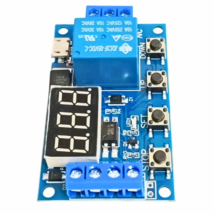
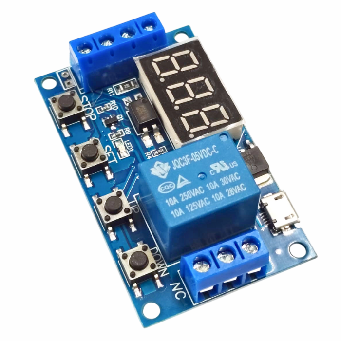
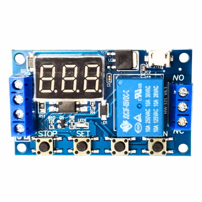
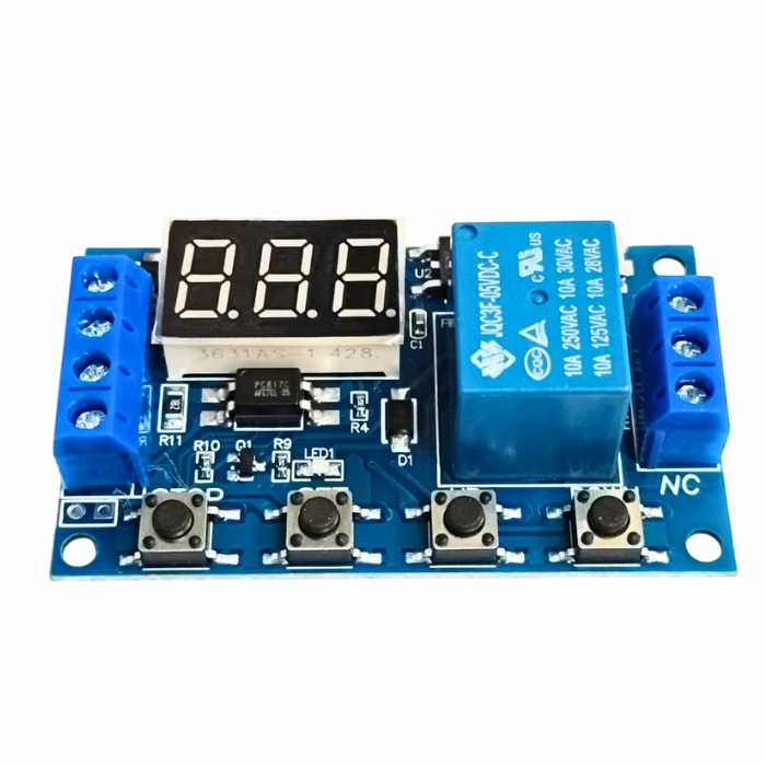
DC 6V To 30V One Way Relay Mo…
DC 6V To 30V One Way Relay Module
Wide voltage power supply (6 - 30v), supports micro usb 5.0v power supply, easy to use.
With emergency stop function (“stop” button) and reverse polarity protection which can avoid burning by reverse connection.
It is 6-30V 1-Channel Delay Power Relay Module with Onboard Adjustable Timing Cycle Switches with Digital LED display It is mostly used in Home Automation Delay Timer Control Switch Module Timer Controller. The Module operates at Operating voltage range of 6-30V, also it supports micro USB 5.0V power supply. Output capability: Can control the device within DC 30V 5A or AC 220V 5A. It can be applied to many fields as there is a wide range of application.
What is Relay
? Explained in simple terms.
Operation Mode:
P1: Trigger signal, the relay is on “OP” time, and then disconnect; Within the “OP” time, proceed as follows:
P1.1: the signal is triggered again, invalid
P1.2: the signal is triggered again, re-clocking
P1.3: Signal has triggered again, the relay is disconnected, stop the clock;
P-2: Trigger signal, after the “CL” time is off, the “OP” time is on. When the timing is completed, the replay will be disconnected;
P3.1: Trigger signal, after the “OP” time is on, the “CL” time is off, then cycle the above actions. If trigger signal within the loop, the relay will be disconnected and stop the clock. The number of cycles ( “LOP “) can be set.
P3.2: No need to trigger the signal after powering up, the “OP” time is on, the “CL” time is off, then cycle the above actions; The number of cycles ( “LOP “) can be set.
P-4: Signal holding function. If the signal is triggered, timing is cleared, the relay remains on; when the signal disappears, the relay will be off when the “OP” time is over; if another signal is triggered during timing, timing will be cleared.
How to choose the time interval:
parameter Introduction: OP power over time, turn off time CL, LOP cycle times (1-999 times, “—” is unlimited cycle)
In the selection of parameter set interface mode, and press the STOP button to select the time.
(1)xxx. if the decimal point is in some place, the time interval is s-1 999 s
(2)xx. x is the decimal place is ten, the time interval is 0.1 s 99.9 s-
(3)x. x. x is the decimal point are all on, the time interval is 1 min-999 min
How to set the parameter:
First, make sure relay operation mode
According to the operating relay mode, the main interface (power module will flash current operating mode; standard mode P1.1, then come into the main interface); long press SET key two seconds and then choose and enter selection interface mode; by pressing UP, DOWN key to choose the mode setting (P1.1 ~ P4)
After selecting the mode, press short SET to set the corresponding parameter, then the parameter you want to set will flash (OP power in time; CL power off time; LOP cycle times, “—” is unlimited cycle ); by UP, DOWN to set the parameter value, support long press (increase or decrease quickly) and press slightly (increase or decrease of 1 unit); after setting the parameter value by short press the STOP key to choosing decimal place; choose the time interval (corresponding time interval is 0.1 s-999 min); Short press SET to set the current mode next parameter, the process is the same as above
After the setting mode parameter, press and hold the SET button then hold the current configuration mode will flash, then go back to the main interface; define success parameter main interface: when the relay does not work, it will show “000” (no decimal point); the operating state relay, the screen has a decimal point
Mode Select Interface:
press and hold the SET key to enter; after setting, long-press the SET button back on the main interface
Activate Relay Mode:
NO: PO in power over time, the relay can be connected
OFF: relay is not allowed to connect, when in the off state
in short main interface press the STOP key to achieve turn ON and OFF, the current state will flash; then back to the main interface
(this function is a function of a sudden stop, 1 key to turn off the relay)
Sleep Mode:
C-P Sleep mode: within 5 minutes, no operation; nixie tube will close auto display, and a function program well
Note:
Press and hold the STOP button for 2 seconds can achieve change from C-P to O-d; Current state will flash and then return to the main interface
The relay contact is passive and electricity production; 1 channel has the control function on / off
₹129,08
Incl. GST (No Hidden Charges)
Out of Stock
MRP. ₹348,60
Incl. GST (No Hidden Charges)
DC 6V To 30V One Way Relay Module
DC 6V To 30V One Way Relay Module Wide voltage power supply (6 - 30v), supports micro usb 5.0v power supply, easy to use. With emergency stop function (“stop” button) …
As low as
₹129,08
₹129,08
MRP. ₹348,60
Incl. GST (No Hidden Charges)
Out of Stock
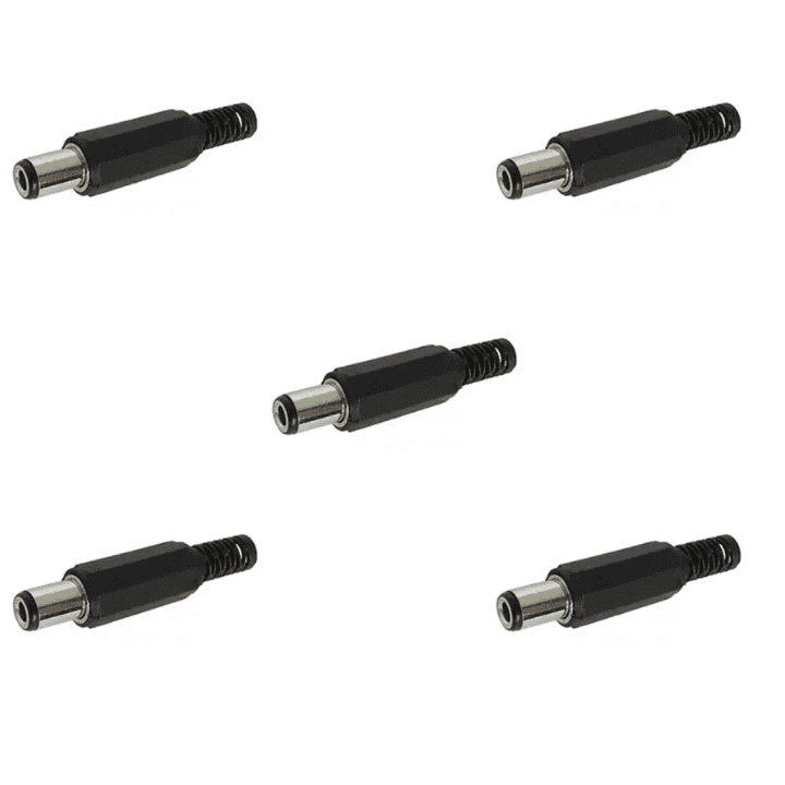
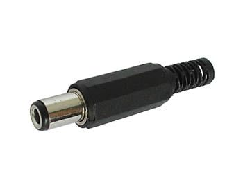


DC Jack Connector with Wire M…
The DC Jack Connector with Wire is a reliable and durable power connection solution designed for a wide range of electronic devices and DIY projects. Featuring a standard 5.5mm outer diameter and 2.1mm inner diameter barrel plug, this connector ensures compatibility with most common power adapters and equipment. The pre-soldered 12-inch (30cm) stranded copper wire with PVC insulation offers excellent conductivity and flexibility, making it ideal for prototyping, repairs, or custom power setups.
Built for performance and safety, this DC jack connector supports up to 2A current and operates efficiently at 12V–24V DC, making it suitable for powering routers, CCTV cameras, LED strips, audio amplifiers, and other low-voltage devices. The robust nickel-plated brass contacts minimize resistance and prevent corrosion, ensuring long-term reliability. Its compact design and secure fit reduce the risk of accidental disconnections, providing stable power delivery in both indoor and light-duty outdoor applications.
Whether you're an electronics hobbyist, technician, or engineer, this DC jack connector simplifies power integration without the need for soldering during installation. It is widely used in Arduino and Raspberry Pi projects, security systems, and portable gadgets. Easy to integrate and highly dependable, this connector is a must-have component for anyone working with DC-powered systems.
₹42,83
Incl. GST (No Hidden Charges)
Out of Stock
MRP. ₹199,00
Incl. GST (No Hidden Charges)
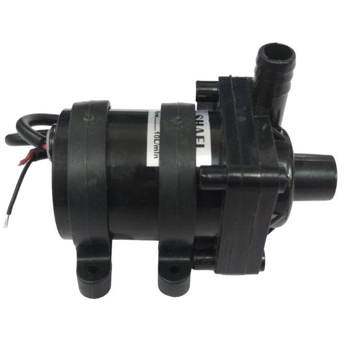
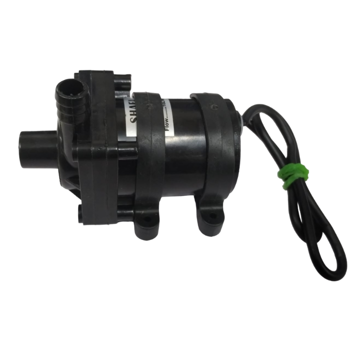
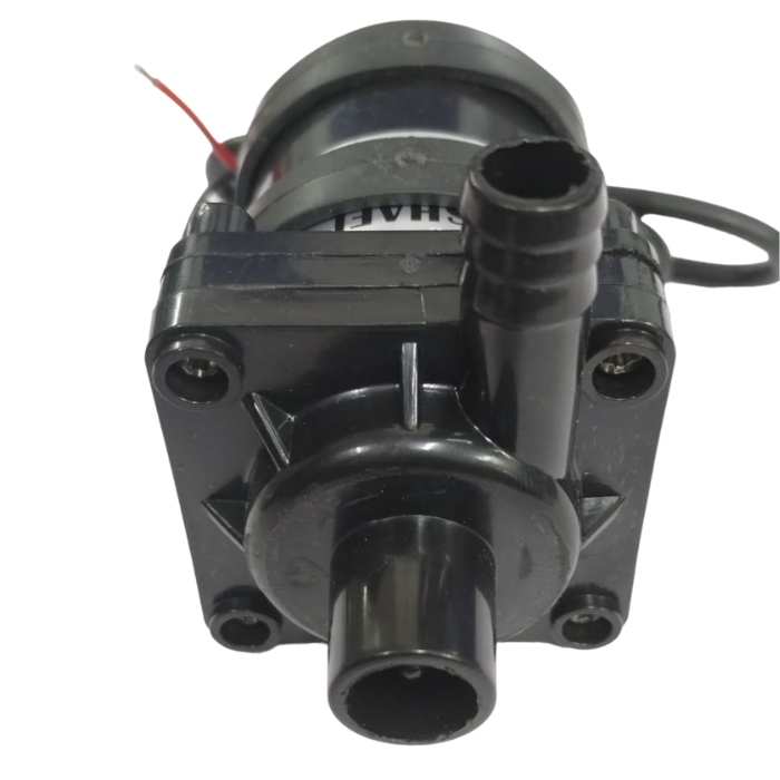
DC Mini Submersible Water Pum…
DC Mini Submersible Water Pump Motor 12V
This DC Mini Submersible Water Pump Motor 12V.The pump can be used with an Aquarium or any other small solar-based pumping application. It can be also used with a Sanitizer Dispenser. This
pump
is completely submersible. DC Powered, can be used in solar systems.
This pump is widely used in industry, scientific research, aerospace industry.
Features:
Bottom inlet design, maximum capacity.
Uses advanced components and wear-resistant shaft
Smooth operation, high efficiency, good performance, long service life
Can be a long time continuously work, low noise,
Applications:
The mini water pump can be used in salt-water or fresh-water
Perfect for small to medium-sized aquariums, fish tanks, pet cat-dog water fountains, waterfalls in terrariums,
Tabletop fountains, spout, and water gardens.
₹313,80
MRP. ₹558,60
Incl. GST (No Hidden Charges)
Incl. GST (No Hidden Charges)


DC Mini Submersible Water Pump Motor 12V
DC Mini Submersible Water Pump Motor 12V This DC Mini Submersible Water Pump Motor 12V.The pump can be used with an Aquarium or any other small solar-based pumping application. It …
As low as
₹313,80
₹313,80
MRP. ₹558,60
Incl. GST (No Hidden Charges)
