

Sort by
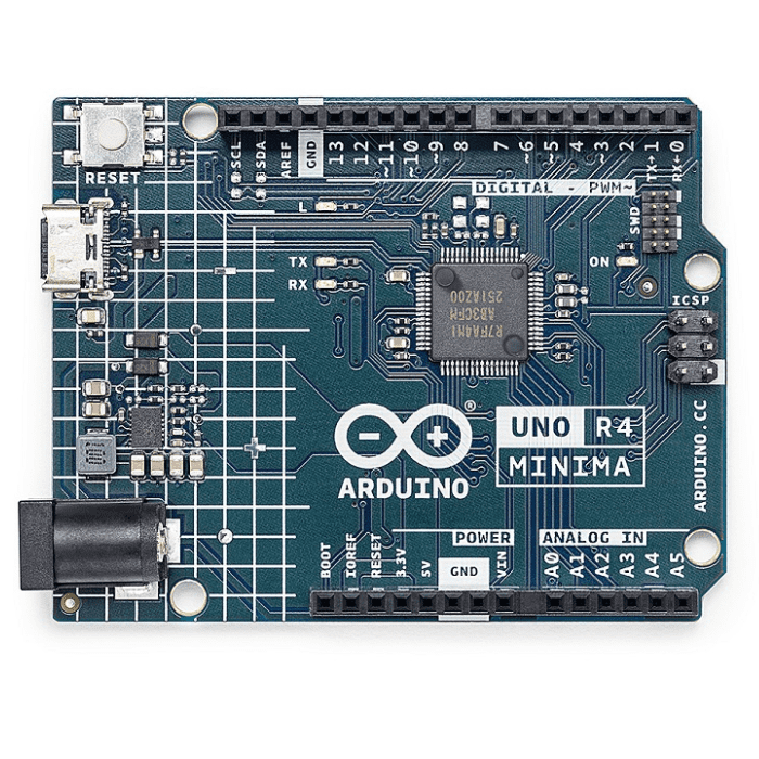
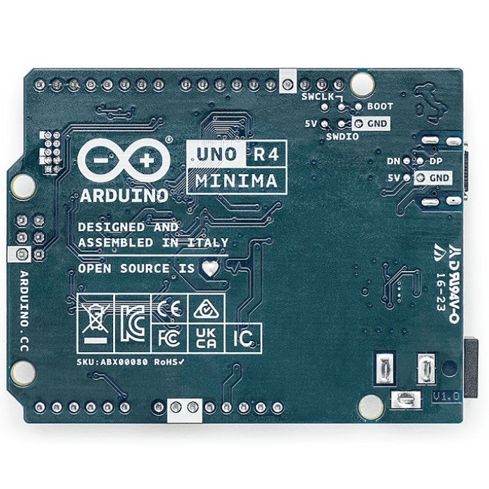
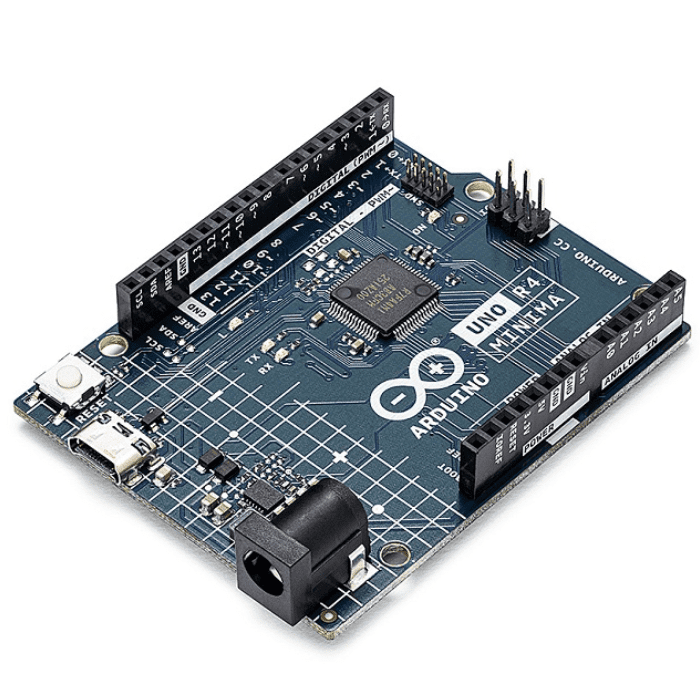
Arduino UNO R4 Minima
Arduino UNO R4 Minima
Presenting the remarkable Arduino UNO R4 Minima, an extraordinary addition to the esteemed UNO board series. This pioneering release showcases an array of impressive attributes, commencing with its utilization of a 32-bit microcontroller.
Empowered by the renowned RA4M1 series microcontroller from Renesas (R7FA4M1AB3CFM#AA0), housing a formidable 48 MHz Arm Cortex-M4 microprocessor.
The UNO R4 Minima presents an expanded capacity for memory, including an impressive 256 kB flash, 32 kB SRAM, and 8 kB of data memory (EEPROM). Operating at 5 V, this board ensures seamless compatibility with UNO form factor accessories tailored for the same voltage.
While earlier UNO shields remain functional, it is important to note that software compatibility may vary due to the microcontroller transition.
Indulge in the unparalleled performance and enriched functionalities of the UNO R4 Minima, and embark on an extraordinary journey of innovation today.
Features:
32-bit development board, previously based on 8-bit AVR
Standard 14 digital I/O ports, 6 analog channels, and dedicated pins for I²C, SPI, and UART connections
Larger memory: 8 times more flash memory (256 kB) and 16 times more SRAM (32 kB)
Easy power management: Barrel jack connector supports input voltages from 6-24 V, eliminating the need for additional circuitry
Cross-compatibility: UNO form factor makes it compatible with existing third-party shields and accessories
Best deals on Original
Arduino UNO R4 WiFi
– Shop now!
Also check out the wide range of Original
Arduino
Boards.
₹1554.50
Incl. GST (No Hidden Charges)
Backorder Available
MRP. ₹2798.60
Incl. GST (No Hidden Charges)
Arduino UNO R4 Minima
Arduino UNO R4 Minima Presenting the remarkable Arduino UNO R4 Minima, an extraordinary addition to the esteemed UNO board series. This pioneering release showcases an array of impressive attributes, commencing …
As low as
₹1554.50
₹1554.50
MRP. ₹2798.60
Incl. GST (No Hidden Charges)
Backorder Available
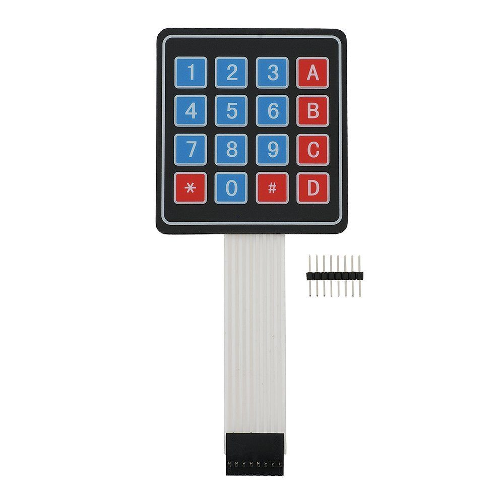
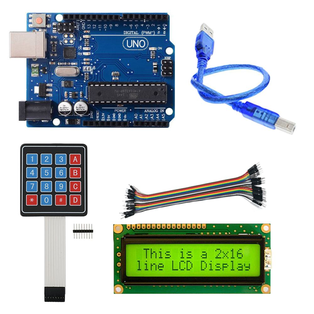
Arduino UNO Robotics Kit comp…
UNO Robotics Kit compatible with Arduino
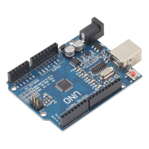
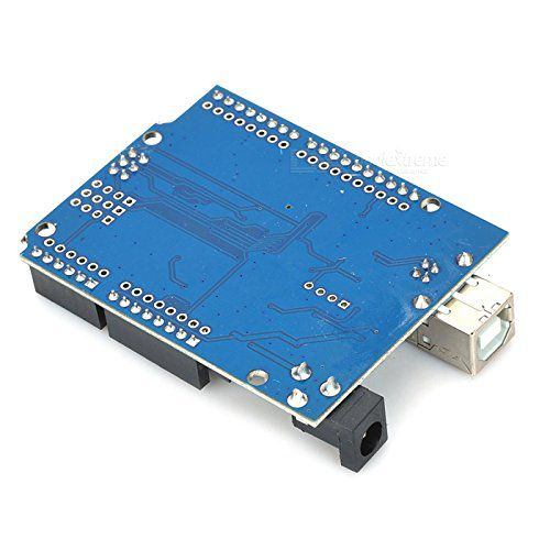
The Arduino basic Starter kit will help you get started in the world of electronics and embedded system programming. This kit is aimed at beginners and can be easily obtained to get you started with DIY electronics Arduino Uno is a microcontroller board based on the ATmega328P. It has 14 digital input/output pins (of which 6 can be used as PWM outputs), 6 analog inputs, a 16 MHz ceramic resonator, a USB connection, a power jack, an ICSP header, and a reset button
This UNO board starter kit is useful for students and hobbyists to test and prototype their electrical projects. Engineering students can buy UNO basic starter kit online to develop and build their final semester projects.
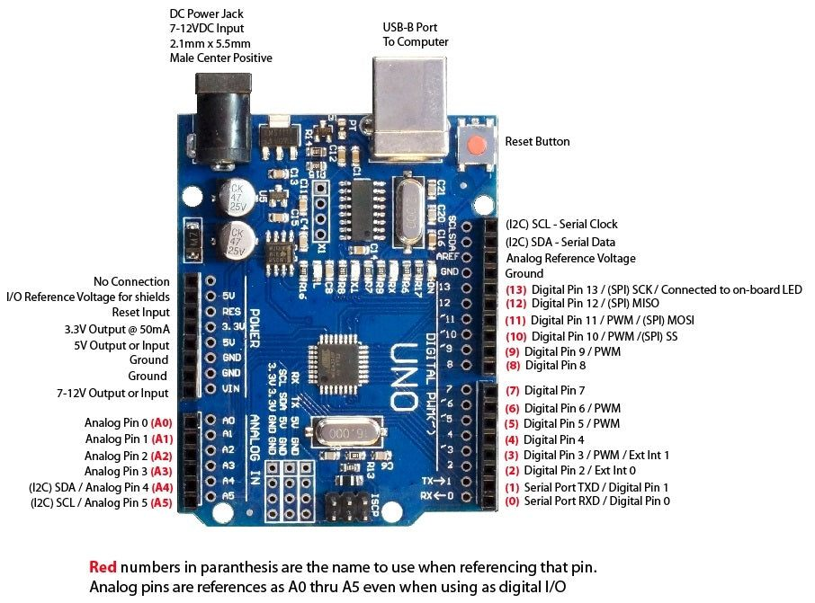
Pinout for Arduino Uno
Pin Diagram of Arduino Uno
Applications:
DIY Projects: This Arduino Uno kit can be used in making fun projects like Keypad operated door lock, ,DIY Calculator etc.
₹722.17
MRP. ₹1748.60
Incl. GST (No Hidden Charges)
Incl. GST (No Hidden Charges)
Arduino UNO Robotics Kit compatible
UNO Robotics Kit compatible with Arduino The Arduino basic Starter kit will help you get started in the world of electronics and embedded system programming. This kit is aimed at …
As low as
₹722.17
₹722.17
MRP. ₹1748.60
Incl. GST (No Hidden Charges)
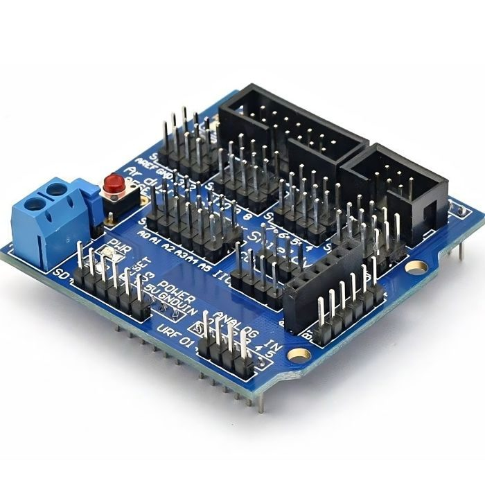
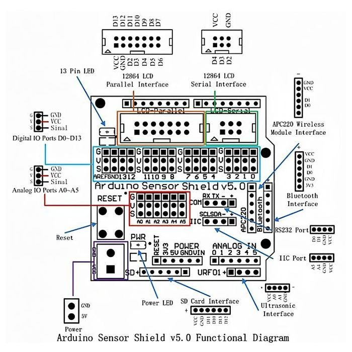
Arduino UNO Sensor Shield Exp…
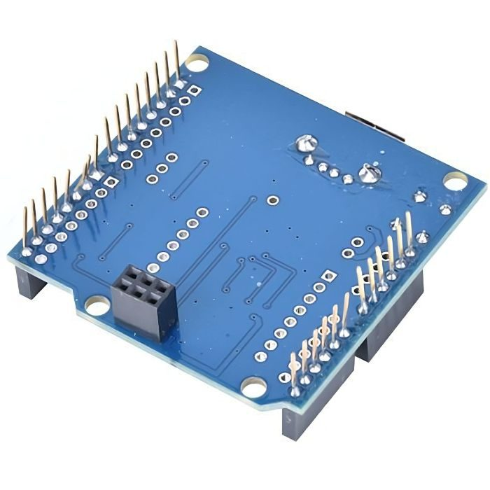
UNO Sensor Shield for Arduino Expansion board V5
This sensor shield for UNO board compatible with Arduino is the latest shield V5 model. This sensor shield allows you to connect to various modules like
sensors
,
servos
,
relays
, buttons,
potentiometers
and many more directly to your
Arduino
through this
Arduino Sensor Shield
. Each functional module has buckled port with VCC, GND, and Output, which has the corresponding port on the Sensor Shield, connected with a plain 2.54mm dual-female cable you may start playing already. Buckled brick cables are like cement for bricks, make the connections easier, secure and more professional looking.
You can easily connect with usual analog sensors by using this expansion board, such as ray sensor. If you support by this expansion board and the corresponding circuit module, you only need to combine Arduino and sensors module by using special cables, because concrete circuit details achieve by corresponding sensors module, so you only need to consider that how to read data coming from the sensor by the program in Arduino.
check out :
Arduino UNO R3, Leonardo Multifunctional Expansion Board
Features:
Laminated design
PCB immersion gold processing technology
IIC interface
Bluetooth module communication interface
SD card module communication interface
APC220 wireless rf modules communication interface
RB URF v1.1 ultrasonic sensors interface
12864 LCD string of line and parallel interface
32 servo controller interface
₹92.36
Incl. GST (No Hidden Charges)
Backorder Available
MRP. ₹180.60
Incl. GST (No Hidden Charges)
Arduino UNO Sensor Shield Expansion board V5
UNO Sensor Shield for Arduino Expansion board V5 This sensor shield for UNO board compatible with Arduino is the latest shield V5 model. This sensor shield allows you to connect …
As low as
₹92.36
₹92.36
MRP. ₹180.60
Incl. GST (No Hidden Charges)
Backorder Available
Arduino UNO SMD compatible Bo…
UNO SMD Board compatible with Arduino
The Uno SMD board is based on the ATmega328. It has 14 digital input/output pins (of which 6 can be used as PWM outputs), 6 analog inputs, a 16 MHz crystal oscillator, a USB connection, a power jack, an ICSP header, and a reset button. It contains everything needed to support the microcontroller; simply connect it to a computer with a USB cable or power it with an AC-to-DC adapter or battery to get started.
The Uno SMD development board comes with a CH340G USB to UART converter chip. So in order to use this board, we need to install the CH340 driver. It can be powered via a USB connection or with an external power supply. The power source is selected automatically.
The AC-DC adapter can be connected by plugging a 2.1mm center-positive plug into the board's power jack. Leads from a battery can be inserted in the Gnd and Vin pin headers of the POWER connector. The board can operate on an external supply of 6 to 20 volts. If supplied with less than 7V, however, the 5V pin may supply less than five volts and the board may be unstable. If using more than 12V, the voltage regulator may overheat and damage the board. The recommended range is 7 to 12 volts.
If you want to use this UNO SMD Board
compatible with Arduino
in your small or DIY projects, for that you will need few essential components like
Breadboards
Jumper wires
batteries or power supply
BO motors
Motor drivers
Sensors
Comparison of Uno Boards:
Specification
UNO Wifi
UNO SMD
UNO R3
Microcontroller
ATmega4809
ATmega328P (SMD)
ATmega328P (Through hole)
USB connector
Micro-USB
USB-B
USB-B
Digital I/O Pins
14
14
14
Analog input pins
6
6
6
PWM pins
5
6
6
UART
Yes
Yes
Yes
I2C
Yes
Yes
Yes
SPI
Yes
Yes
Yes
I/O Voltage
5V
5V
5V
Input voltage (nominal)
7-12V
7-12V
7-12V
DC Current per I/O Pin
20mA
20 mA
20 mA
Power Supply Connector
Barrel Plug
Barrel Plug
Barrel Plug
clock speed
16 MHz
16 MHz
16 MHz
USB-Serial chip
ATmega16U2
CH340
ATmega16U2
SRAM
6.144KB
2KB
2KB
Flash Memory
48KB
32KB
32KB
EEPROM
256 Bytes
1KB
1KB
Dimensions
68.6 mm x 53.4 mm
68.6 mm x 53.4 mm
68.6 mm x 53.4 mm
RADIO MODULE
u-blox NINA-W102
-
-
Inertial Measurement Unit
LSM6DS3TR (3D accelerometer)
-
-
LED_BUILTIN
25
13
13
Wi-Fi Microprocessor
Yes
-
-
Applications:
Arduino Music Instrument
Robot Car
Fingerprint door lock
Home Automation
Security systems
₹8962.01
Incl. GST (No Hidden Charges)
Backorder Available
MRP. ₹17465.00
Incl. GST (No Hidden Charges)
Arduino UNO SMD compatible Board(Pack of 25)
UNO SMD Board compatible with Arduino The Uno SMD board is based on the ATmega328. It has 14 digital input/output pins (of which 6 can be used as PWM outputs), …
As low as
₹8962.01
₹8962.01
MRP. ₹17465.00
Incl. GST (No Hidden Charges)
Backorder Available
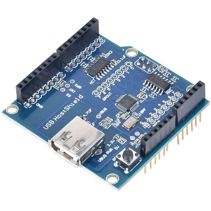
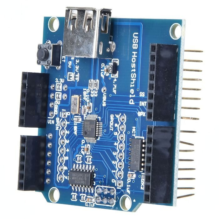
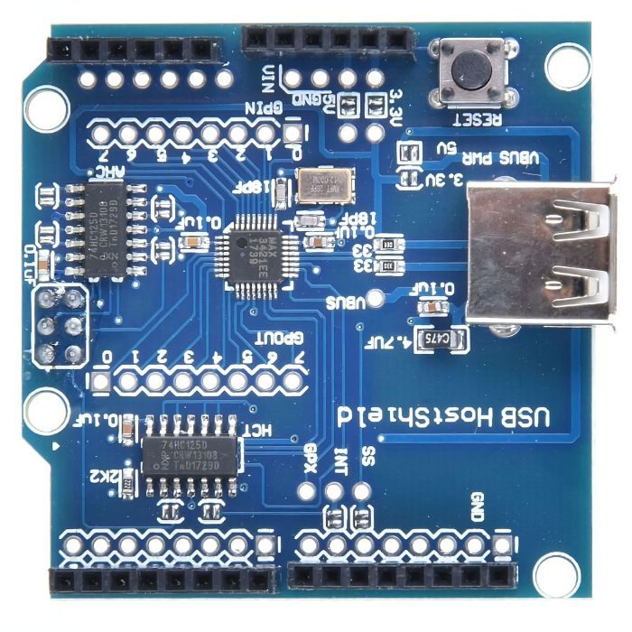
Arduino UNO USB Host Shield
UNO USB Host Shield for Arduino
The UNO USB Host Shield
compatible with Arduino
is based on the MAX3421E, which is a USB peripheral/host controller containing the digital logic and analog circuitry necessary to implement a full-speed USB peripheral or a full-/low-speed host compliant to USB specification rev 2.0. For a successful communication to happen using USB host shield protocol, you need at least one of the device to be the host, which means that you cannot connect two keyboards together and expect them to communicate with each other.
Features:
Works with standard (dual 5/3.3V) and 3.3V-only (for example, Pro Arduino) boards.
Operates over the extended -40°C to +85°C temperature range
Complies with USB Specification Revision 2.0 (Full-Speed 12Mbps Peripheral, Full-/Low-Speed 12Mbps/1.5Mbps Host)
Supports HID devices, such as keyboards, mice, joysticks, etc.
Compatible with Mass storage devices, such as USB sticks, memory card readers, external hard drives
Applications:
Interfacing HID Devices: Connects keyboards, mice, and joysticks to Arduino projects.
Game Controllers: Allows the use of Sony PS3, Nintendo Wii, and Xbox360 controllers with Arduino.
USB to Serial Converters: Supports FTDI, PL-2303, ACM, and certain cell phones and GPS receivers.
Android Devices: Enables communication with ADK-capable Android phones and tablets.
Digital Cameras: Interfaces with Canon EOS, Powershot, Nikon DSLRs, and other PTP cameras.
Mass Storage Devices: Connects USB sticks, memory card readers, and external hard drives.
Bluetooth Dongles: Adds Bluetooth connectivity to Arduino projects.
Custom USB Controllers: Create custom USB controllers for various applications.
Data Logging: Log data from USB devices like sensors and storage devices.
Robotics: Integrate USB peripherals into robotics projects for enhanced functionality.
₹645.39
MRP. ₹1398.60
Incl. GST (No Hidden Charges)
Incl. GST (No Hidden Charges)
Arduino UNO USB Host Shield
UNO USB Host Shield for Arduino The UNO USB Host Shield compatible with Arduino is based on the MAX3421E, which is a USB peripheral/host controller containing the digital logic and …
As low as
₹645.39
₹645.39
MRP. ₹1398.60
Incl. GST (No Hidden Charges)
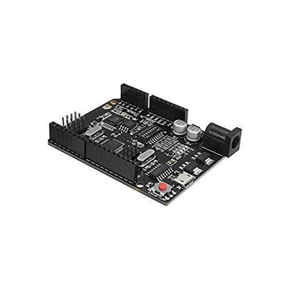
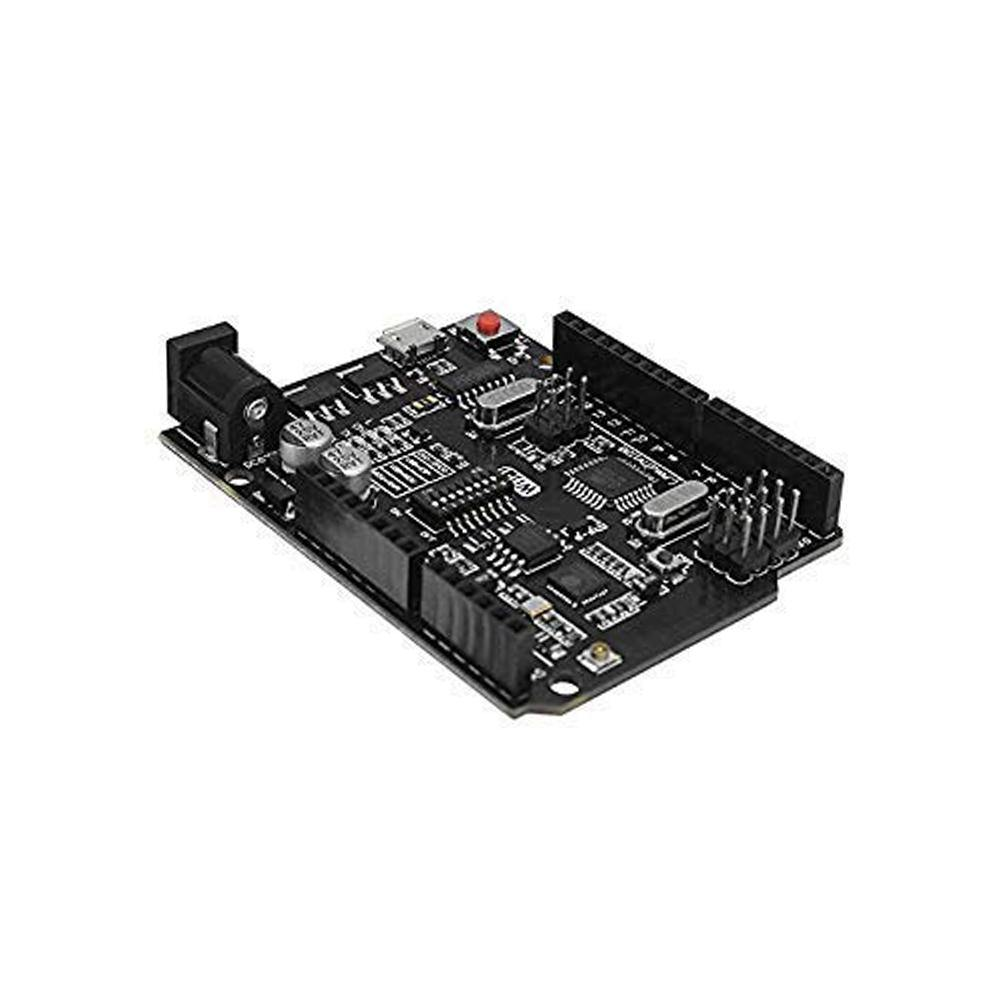
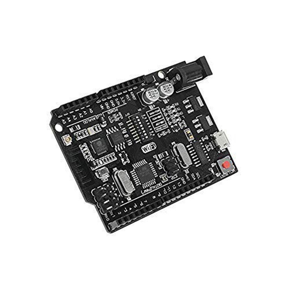
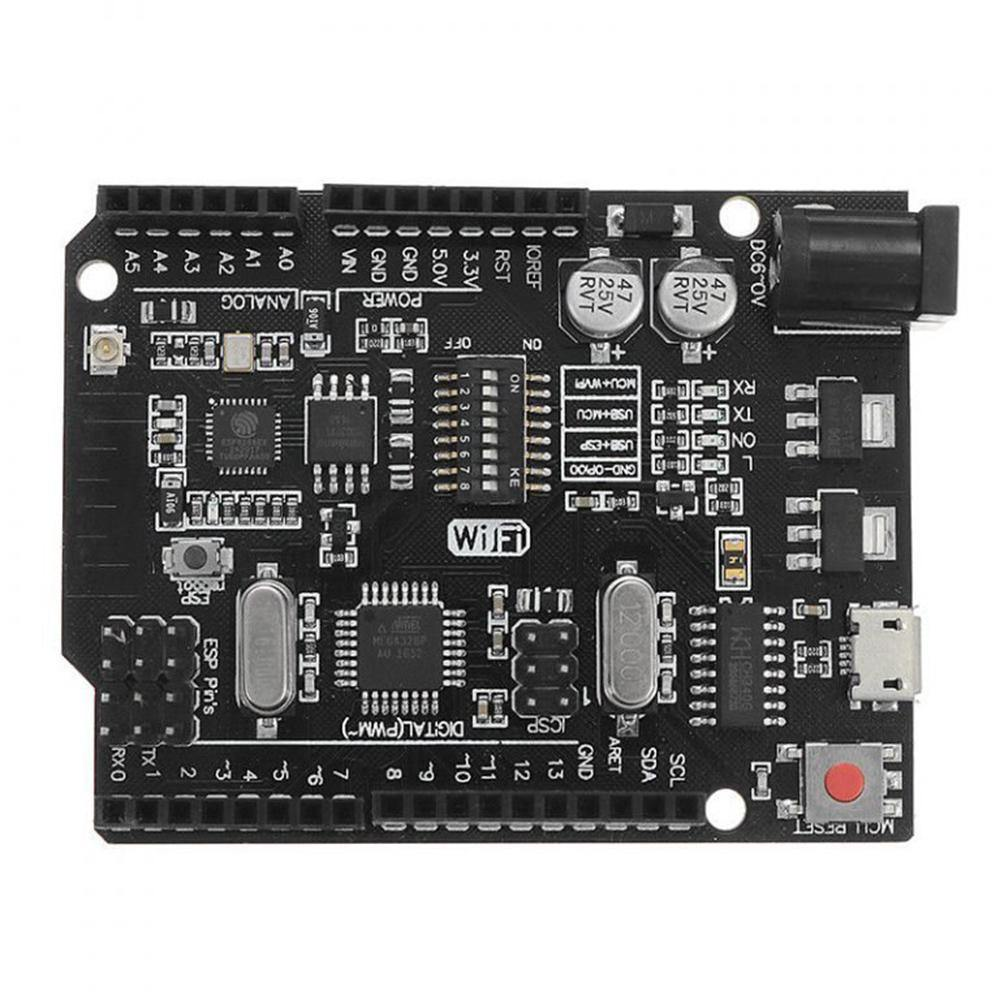
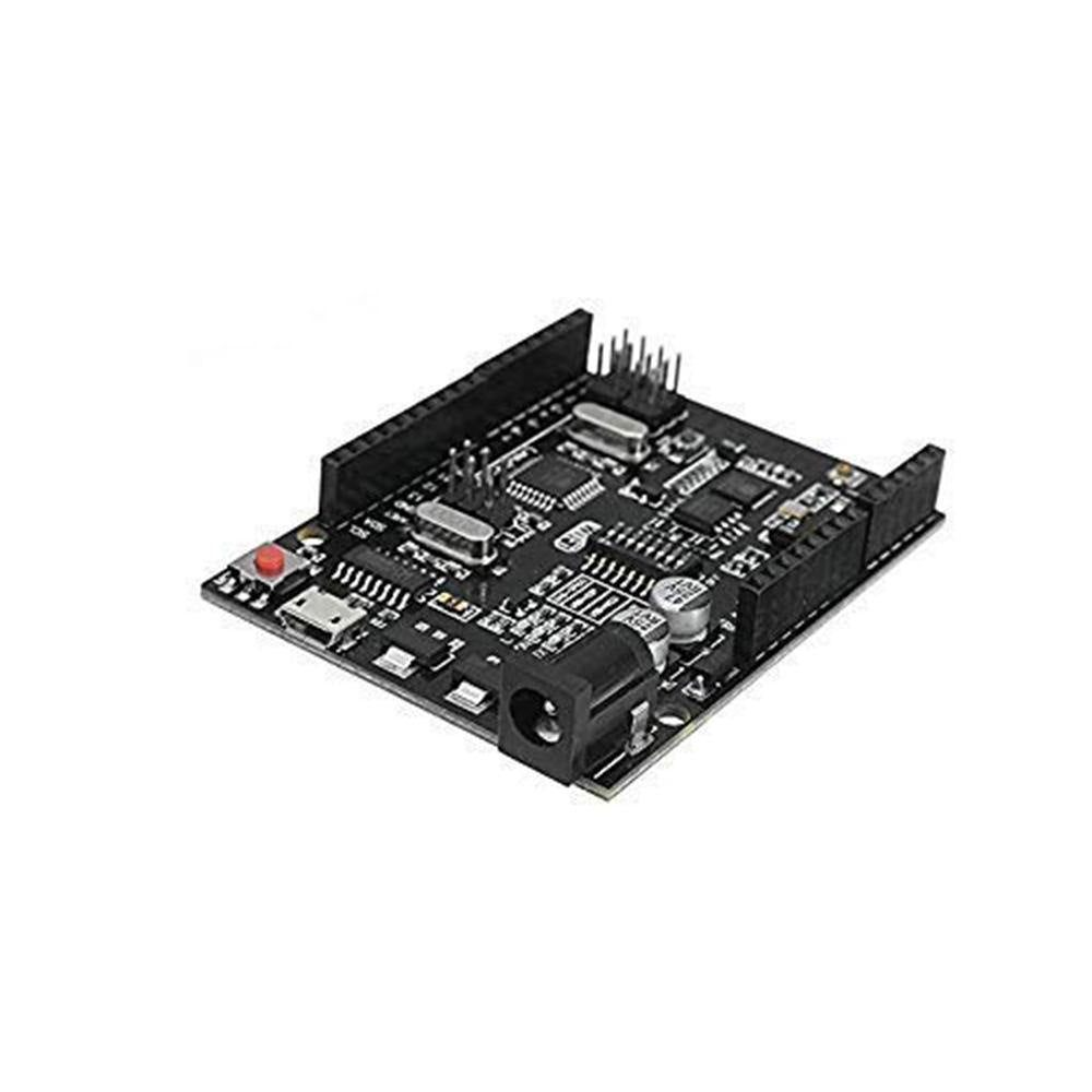
Arduino UNO+WiFi R3 ATmega328…
CH340G Board compatible with Arduino
The Uno+WiFi R3 is a fully integrated board that combines the Uno R3 ATmega 328 microcontroller with the WiFi ESP8266 chip, along with 8Mb of memory, all on a single board. Both modules can operate together or separately, each with their own pinout headers.
This board provides a convenient solution for developing new projects that require both Uno and WiFi functionalities. It includes a USB-serial converter, CH340G, allowing for easy updating of sketches and firmware for both ATmega328 and Node MCU ESP8266.
Essentially a modernized version of the classic Arduino UNO R3 board, the Uno+WiFi R3 offers simple operations and includes a DIP switch to connect the different modules in various configurations. LED lights are provided for connecting peripheral sensors and modules, making it a versatile choice for a wide range of projects.
Check out the entire range of
Compatible Arduino Boards
Applications:
WiFi-based IoT applications.
IoT home automation.
Internet Smoked Alarm.
Incubator Controller.
Security Alarms.
Comparison With Similar Boards:
Specification
UNO Wifi
UNO SMD
UNO R3
Microcontroller
ATmega4809
ATmega328P (SMD)
ATmega328P (Through hole)
USB connector
Micro-USB
USB-B
USB-B
Digital I/O Pins
14
14
14
Analog input pins
6
6
6
PWM pins
5
6
6
UART
Yes
Yes
Yes
I2C
Yes
Yes
Yes
SPI
Yes
Yes
Yes
I/O Voltage
5V
5V
5V
Input voltage (nominal)
7-12V
7-12V
7-12V
DC Current per I/O Pin
20mA
20 mA
20 mA
Power Supply Connector
Barrel Plug
Barrel Plug
Barrel Plug
clock speed
16 MHz
16 MHz
16 MHz
USB-Serial chip
ATmega16U2
CH340
ATmega16U2
SRAM
6.144KB
2KB
2KB
Flash Memory
48KB
32KB
32KB
EEPROM
256 Bytes
1KB
1KB
Dimensions
68.6 mm x 53.4 mm
68.6 mm x 53.4 mm
68.6 mm x 53.4 mm
RADIO MODULE
u-blox NINA-W102
-
-
Inertial Measurement Unit
LSM6DS3TR (3D accelerometer)
-
-
LED_BUILTIN
25
13
13
Wi-Fi Microprocessor
Yes
-
-
₹533.01
MRP. ₹1048.60
Incl. GST (No Hidden Charges)
Incl. GST (No Hidden Charges)
Arduino UNO+WiFi R3 ATmega328P+Node MCU ESP8266 CH340G Compatible Board
CH340G Board compatible with Arduino The Uno+WiFi R3 is a fully integrated board that combines the Uno R3 ATmega 328 microcontroller with the WiFi ESP8266 chip, along with 8Mb of …
As low as
₹533.01
₹533.01
MRP. ₹1048.60
Incl. GST (No Hidden Charges)
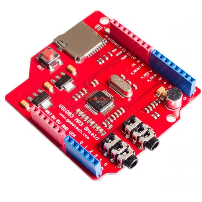
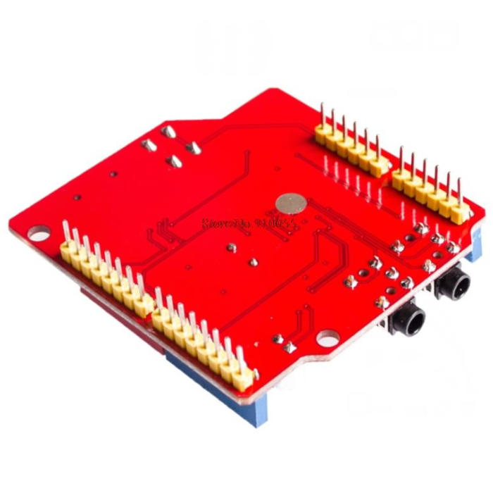
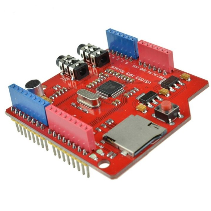
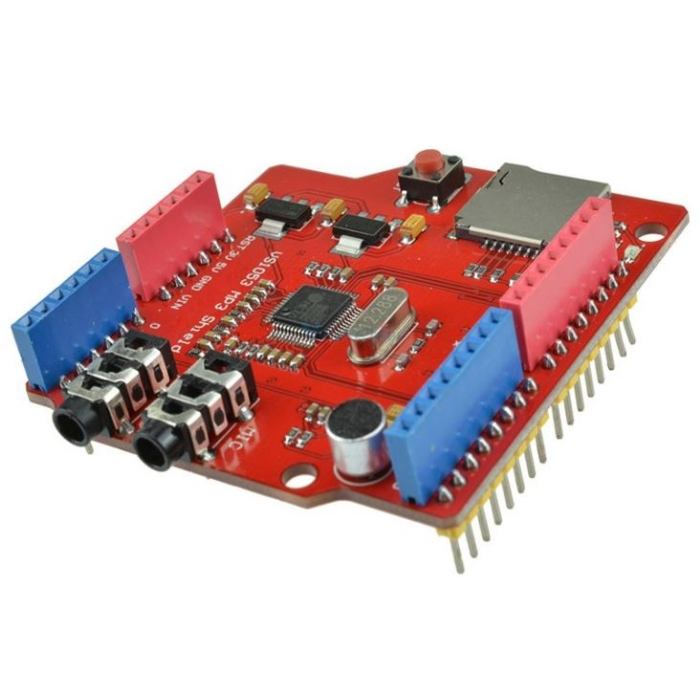
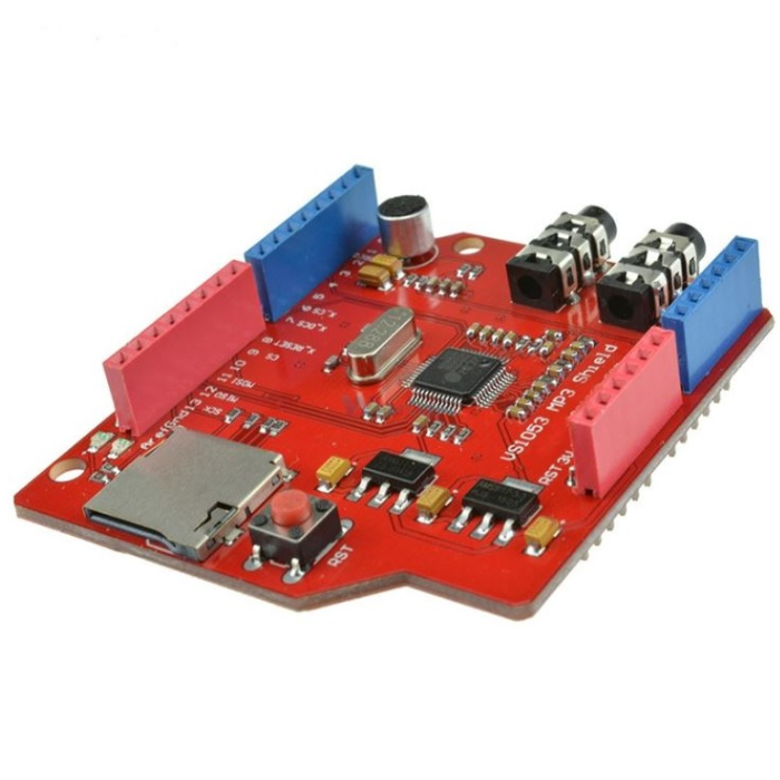
Arduino VS1053 MP3 Shield
VS1053 MP3 Shield for Arduino
This VS1053 MP3 Shield for Arduino with onboard recording function can record and playback a variety of music formats, and support for OGG encoding real-time recording.
VS1053 is in addition to playing a variety of music formats but also supports the OGG real-time encoding recording. SPI interface, and control signal lines are extracted. The VS1053 MP3
Shield for Arduino
has an onboard TF SD card slot to store the record data as well as playback whenever you want, or you can easily transport the recorded MP3 file to any device via SD card.
The MP3 shield module has two separate 3.5 mm jacks for audio Out & Microphone In and Onboard Microphone for recording. This MP3 shield has a capacitor filter and a 12.288Mhz crystal oscillator and with an onboard power indicator light, it easy to monitor the on/off status of the module. Also, the onboard 3.3V and 2.5V LDO chip AMS-1117 provide 800mA current. The single power supply onboard for +5VDC provides the constant stabilized voltage to the circuit.
read more :
VS1053 MP3 Shield with Arduino Uno
Features:
SPI interface, the control signal lines are led out
A headphone and stereo output
Onboard Microphone for recording
A line-in input interface
Separate 3.5 mm Jack for MIC and Speaker
Onboard Power Indicator 3.3V and 2.8V of LDO chip AMS-1117 on board provides up to 800mA current
Can play a variety of music formats, support for OGG encoding real-time recording
TF card slot
Applications:
DIY MP3 Players: Create custom MP3 players with playback and recording capabilities.
Sound Effects for Projects: Add sound effects to interactive projects like haunted houses or Halloween costumes.
Voice Recorders: Build voice recording devices for various applications.
Audio Playback in Robotics: Integrate audio playback in robotic projects for voice commands or feedback.
Educational Tools: Develop educational tools that use audio for instructions or feedback.
Home Automation: Use in-home automation systems to provide audio alerts or notifications.
Interactive Art Installations: Enhance art installations with soundscapes or interactive audio elements.
₹876.83
MRP. ₹1398.60
Incl. GST (No Hidden Charges)
Incl. GST (No Hidden Charges)
Arduino VS1053 MP3 Shield
VS1053 MP3 Shield for Arduino This VS1053 MP3 Shield for Arduino with onboard recording function can record and playback a variety of music formats, and support for OGG encoding real-time …
As low as
₹876.83
₹876.83
MRP. ₹1398.60
Incl. GST (No Hidden Charges)
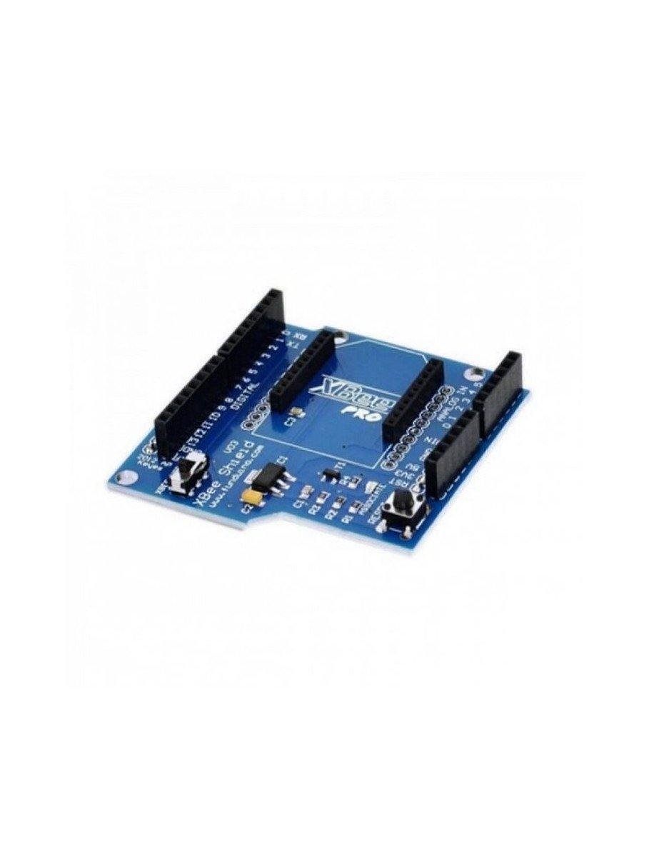
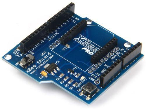
Arduino xBee Shield
xBee Shield for Arduino
xBee shield Modules are great for long range wireless communications and to implement complex mesh networks. But using them in your projects has always been difficult because of the xBee modules odd pin spacing, voltage regulator and level shifter requirements. This shield simplies these issues and makes using xBee Modules almost plug and play. Using this shield, you only have to insert your xbee module on the provided socket and plug the
Arduino shield
onto your UNO board
compatible with Arduino
. With no additional circuit and connections required, you can then start using the xbee modules.
This Xbee Shield allows boards compatible with Arduino to communicate wirelessly with each other using Zigbee. This module works with all Xbee module including Zigbee Series 1, Zigbee Series 2 and also Xbee Pro versions. Whats great it also works with Bluetooth bee Modules.
Onboard slide switch lets you connect the xbee DIN and DOUT lines to the microcontrollers compatible with arduino or the USB Port. This means you can use your xBee to communicate with the Arduino or the computer. You can communicate with the computer to program the xbee modules using the XCTU software. Features:
Shield lets you use the xbee modules with boards compatible with arduino without the need for any external components or connections
Greatly simplifies using xbee modules and offers plug and play interface
Any XBee module will work with the shield.
Also check
XBEE USB Explorer
. It is a versatile board designed to simplify the connection of XBee modules to a computer. The board features a FT231X USB-to-Serial converter for seamless data translation between the computer and the XBee module. It includes four LEDs for debugging (RX, TX, RSSI, and power indicator), a reset button, and headers compatible with breadboards.
₹159.12
MRP. ₹278.60
Incl. GST (No Hidden Charges)
Incl. GST (No Hidden Charges)
Arduino xBee Shield
xBee Shield for Arduino xBee shield Modules are great for long range wireless communications and to implement complex mesh networks. But using them in your projects has always been difficult …
As low as
₹159.12
₹159.12
MRP. ₹278.60
Incl. GST (No Hidden Charges)
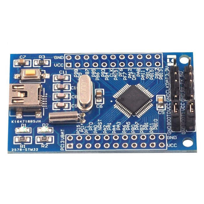
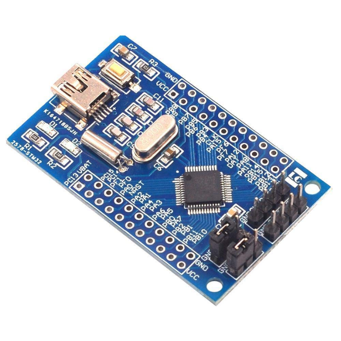
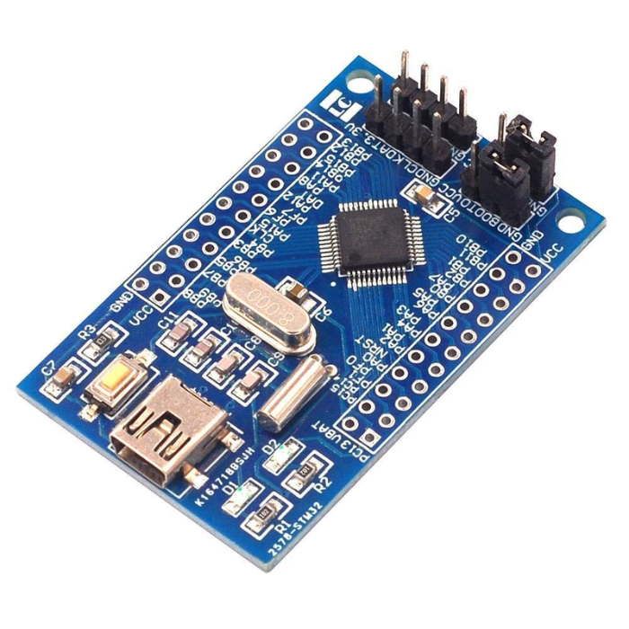
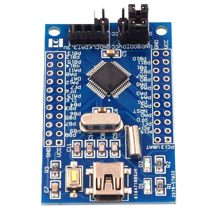
ARM Cortex-M0 STM32F051C8T6 S…
ARM Cortex-M0 STM32F051C8T6 STM32 Core Board Minimum Development Board
Check out our newest product, the Cortex-M0 STM32F051C8T6 ARM Core Board Development Board. It's created for everyone who appreciates making art, regardless of level of experience.
This board features a strong Cortex-M0 processor, enough of storage capacity, and a steady clock to keepeverything going smoothly. It's ideal for creating devices, testing out new ideas, and learning about electronics.
The SWD debug download tool allows you to easily resolve any issues with your projects and requires only a Mini-USB cord to get started. Made by FlyNoval, you can be confident that it will work every time. Begin your adventure into interesting projects with the Cortex-M0 STM32F051C8T6 ARM Core Board, currently available at Iotcart. Let your creativity fly!
₹792.28
MRP. ₹1397.20
Incl. GST (No Hidden Charges)
Incl. GST (No Hidden Charges)

ARM Cortex-M0 STM32F051C8T6 STM32 Core Board Minimum Development Board
ARM Cortex-M0 STM32F051C8T6 STM32 Core Board Minimum Development Board Check out our newest product, the Cortex-M0 STM32F051C8T6 ARM Core Board Development Board. It's created for everyone who appreciates making art, …
As low as
₹792.28
₹792.28
MRP. ₹1397.20
Incl. GST (No Hidden Charges)
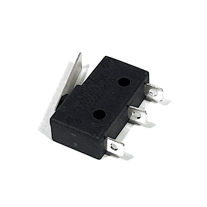
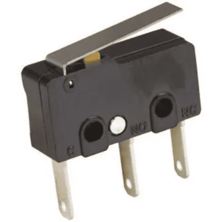
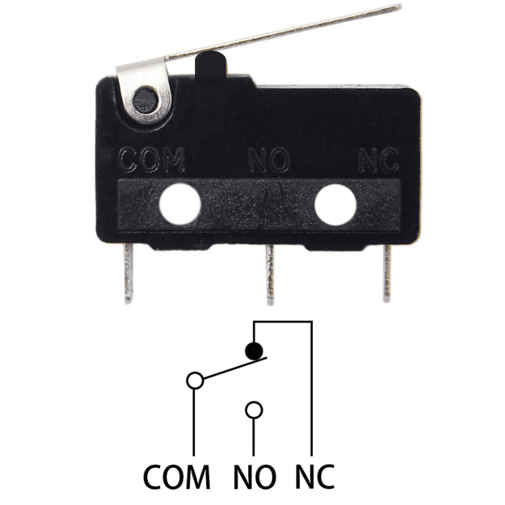
Arm Lever 15mm, 250V 6A SPDT …
Arm Lever 15mm, 250V 6A SPDT 3-Pin Momentary Plastic Micro Limit Switch
This is an Arm Lever 15mm, 250V 6A SPDT 3-Pin Momentary Plastic Micro Limit Switch Incorporating a snapping mechanism made with two highly precise split springs that ensure long durability. Using insertion of molded terminals that prevent flux penetration. In addition to self-clinching PCB, left-angled, and right-angled terminals, 2 types of soldering terminals are available. It has a Lineup of 5A types for high-load applications.
₹50.08
Incl. GST (No Hidden Charges)
Backorder Available
MRP. ₹96.60
Incl. GST (No Hidden Charges)
Arm Lever 15mm, 250V 6A SPDT 3-Pin Momentary Plastic Micro Limit Switch
Arm Lever 15mm, 250V 6A SPDT 3-Pin Momentary Plastic Micro Limit Switch This is an Arm Lever 15mm, 250V 6A SPDT 3-Pin Momentary Plastic Micro Limit Switch Incorporating a snapping …
As low as
₹50.08
₹50.08
MRP. ₹96.60
Incl. GST (No Hidden Charges)
Backorder Available
